• Hello MLAers! We've re-enabled auto-approval for accounts. If you are still waiting on account approval, please check this thread for more information.

ProtoCache1 - IIsi/SE/30 PowerCache Adapter Prototype Development

ALLPCB it is then! They were always the lowest quote and so at the front of my mind. Lowest quality/lowest yield doesn't matter a bit even if that's the case. The layout is super simple compared to what all the board houses deal with every day. Between one and three good boards out of the batch needed max.

These will be an order of magnitude easier to implement and far more reliable during testing. I was ready to make do with just the one fully wrapped protoboard in the IP:

/monthly_05_2017/post-902-0-76475600-1495680303.jpg">View attachment 12863

This is a lot more convenient and for not a whole lot of money! [:D] ]'>

ProroCache2.JPG

I'd say it's been time well spent, now to splay a simplified version of the layout across four layers.

 
Last edited by a moderator:
ALLPCB shouldn't be too bad even so, they are ISO 9001 certified.

Would you like me to prepare some gerbers based on the documents you just posted?

I'll see what I can do tomorrow, before I leave on vacation.

 
Last edited by a moderator:
Well, more like 13 pages, but some of those pages don't have public hits ;)

I'll probably get started on producing gerbers for you (tomorrow, after I have caffeinated my body), so you don't have to wait for me being on vacation :D

If you decide you don't need/want them right now, let me know.

 
Last edited by a moderator:
Nah, way too soon to start all that. I've gotta work out the traces, Power & Ground all over again making use of all four layers.

There's one thing you could do now that would be a big help though. Set up the text for pin numbers for MB CI and PDS along with the pinout for the area between MB and its combination wire wrap pin breakout/PDS test connector on the silk screen layer so I can see how it'll look. Laying in all the holes for the connectors and wire wrap pins as they stand would be great too. I can use your work as a template in Illustrator one way or another to play around with while you're on vacation.

If I need to move connectors or pins around that'll be easy to change. Biggest concern there would be whether or not I need to move the components above the daughtercard headers farther away from the mounting bracket for connector clearance.

 
Don't infer lack of postings as no interest! I've been following very closely, but don't know enough to contribute. I'm not much of a cheerleader either!
Thank you very much Joe! It doesn't surprise me that folks are hesitant to contribute to something that they don't really know much about. They just understand that this will let them accelerate their 030 PDS based mac!

 
This looks interesting, but I'm confused as to exactly what you're building. Is there a summary or overview somewhere?

FYI, I ordered some small 2-layer PCBs from ALLPCB a few weeks ago, and a couple of days later my credit card had a bunch of fraudulent charges. I don't know if it's related, but I'm suspicious. But the PCBs themselves came out fine.

 
I'm confused as to exactly what you're building. Is there a summary or overview somewhere?
It's supposed to be a clone of the PowerCache.

Have you ever heard of the Artmix TwinSpark adaptor? (If you don't read Japanese, run it through Google Translate) This is designed to be functionally identical to it. Not really a proper clone, but similar. There are a few other adaptors that let you plug in accelerators designed for the IIci cache slot into the SE/30 or the IIsi, and this is going to be one of them.

Another Example:

2406671347_48595e7c7f_z_d.jpg.13a4a735508784b6f4c8c1e08401799c.jpg


Last edited by a moderator:
I'm documenting the prototyping phase of my attempt to complete the PowerCache Adapter cloning project Gamba & Company abandoned. I was going to do a standard wire wrap prototype on perf board as in the pic in the IP. Themk pitched in to do some PCB design and it got a bit out of hand. [:)] ]'>

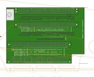
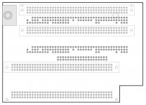
The side view pretty much explains the layout. It's a custom PCB for wire wrap prototyping PowerCache Adapters for the IIsi and SE/30.

PDS - Top connector is for the PDS passthru with address/data/control lines leap-frogged from the IIci Cache slot adaptation. It's configured for standard or RA connectors.

\

/

wire wrap connectors for CI - OUT

|

CI - soldered IIci Cache Slot connector with traces

|

wire wrap connectors for CI - IN

\

/

2x20 header for wiring up the GAL on a daughtercard - some lines detour here and back out to the main board

\

/

PDS - TEST - this was to be wire wrap headers, but switched to a wire wrap PDS passthru socket for testing purposes

|

Bottom connector plugs into PDS

|  =  copper traces

\

/  =  wires wrapped between sections, they're meant to keep trace lengths as close to equal as possible. Laying out a multilayer board for keeping the traces equal befoer doing a proof of concept would be inadvisable, so wire wrap is the way to go for the time being.

Only a handful of lines will detour onto the daughtercard, but the total lengths of these purple wires and related traces should equal the direct connections, which will be matched to the adaptation spec.

I hope that explains it? I'm glad you popped in. I was going to get in touch with you about adding line drivers/buffers to the card if we get it up and running. The 030 PDS isn't capable of driving more than the single passthru found on all the adapters I've seen out there. Gotta make use of all those lovely Slot IDs!  [}:)] ]'>

 
Last edited by a moderator:
PC2-Alpha-200-SS.JPG

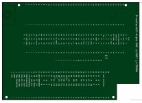
I haven't checked the IIci Pinout copy (forgot even to check if A& C rows are reversed) but it's full width Andale Mono @ 1mm height, hope it matches the KiCAD face closely enough in width. I had to munge the connectors about and slide the text around in between a bit to get the copy to fit. Not necessary, but having all the signals for PDS and Cache silk screened on the board along with the full pin# lists will be most helpful. Wrapping on blank perfboard is the pits.

PC2-Alpha-200-Drill list.JPG

Not really a complete drill list, but this shows the board with a lot less confusion than the usual stuff I print out for playtime at work.

ProtoCacheII-AlphaSS-200.PDF

PC2-Alpha-SS-Drill.200.PDF


Attachments

Last edited by a moderator:
I think there's a lot of backstory here that I was missing that might be obvious to everyone else. Here's my attempt to summarize, please correct me where I'm wrong:

  • Daystar Powercache is a product line of '030 and '040 CPU accelerators designed to directly fit the PDS slot of a Mac II, IIx, IIci, or IIcx.
  • The Powercache can also be used in the PDS slot of a IIsi or SE/30, but requires an adapter. (Why is an adapter required? Is the PDS slot physically different, or is it just a straight-through 90-degree adapter so that the Powercache board will fit inside the case?)
  • You're not cloning the Powercache itself, you're cloning the Powercache *adaptor* because they're rare and hard to find.
  • Your adapter will also have two separate PDS pass-through connectors on it, in addition to the Powercache connector.
What do the GAL and other electronics on the board do? Some kind of muxing of address lines?

JT mentioned a daughtercard - where is that? I didn't see it in the mockups. Why is a daughtercard needed?

If I've understood correctly, then I wouldn't necessarily assume you need anything more than a 2-layer board here. Sure there are a lot of pins on those connectors, but I assume most of them are just connected straight to the matching pins on the neighboring connector, so it should be fairly easy to route the traces. It's probably at least worth a try. 2 layer boards will be a little cheaper, and are easier to debug than 4+ layer boards, since you can always cut a trace or add a patch wire if you find little mistakes in the PCB design. 

I also wouldn't think you need to worry too much about matching the trace lengths. This board will be carrying signals at what - 25 MHz? Or whatever the bus speed is? I may be wrong, but I've always viewed matched trace lengths as a concern for designs running at hundreds of MHz or more, like fast SDRAM interfaces. I've never worried about trace lengths in anything I've designed, since all my stuff runs at a few tens of MHz or less.

Random note: I once found one of those PDS adapters in a IIsi that I bought. I didn't really know what to do with it, and I think I ended up giving it away to someone.

 
Last edited by a moderator:
Hey Trash and Themk

I like the idea of the proto boards.  The flexibility is most important to me.  But what about the issue of resistance? I thought the purpose of the big board was to unify all the signals.  Anyway I support what you are doing see you breathing new life into the SE/30, keep up the good work.

tpope

 
I think there's a lot of backstory here that I was missing that might be obvious to everyone else. Here's my attempt to summarize, please correct me where I'm wrong:
  • Daystar Powercache is a product line of '030 and '040 CPU accelerators designed to directly fit the .  .  .
The accelerators we're talking about are DayStar's Univesal PowerCache models that were made to only support the IIci Cache Slot directly. All other supported Macs required adapters, passive or active to adapt their I/O to the IIci Cache Slot interface. Mostly 030 CPU PDS slots, but also the Mac II's 020/MMU sockets and the IIx and IIcx 030 Sockets were all converted to the Cache Slot spec. in order to use these accelerators.

The Powercache can also be used in the PDS slot of a IIsi or SE/30, but requires an adapter. (Why is an adapter required?
Yes, the SE/30 and IIsi require electrically compatible active adapters to convert their common 030 PDS into a IIci Cache Slot, which is an entirely different beast. Plugging either a PDS or Cache card into the others slot releases the magic smoke. Power and Ground pins vary greatly across the two interfaces

You're not cloning the Powercache itself, you're cloning the Powercache *adaptor* because they're rare and hard to find.
Yep, just the adapters, greatest demand will be for SE/30 adapters with some for the IIsi. But hopefully we'll get the adaptation worked out for the full range of Macs that DayStar supported.

Your adapter will also have two separate PDS pass-through connectors on it, in addition to the Powercache connector.
Yes, all adapters so far have been limited to a single passthru. Likely because the PDS lines are spec'd to drive only two inputs. This is an affront to my expansionist sensibilities. I'd love to drive inputs for making use of all three interrupts along with the PowerCache if at all possible.

What do the GAL and other electronics on the board do? Some kind of muxing of address lines?
I've heard another theory and been told mine's in error, but I'm sticking to it! I've done a pretty thorough analysis I'm pretty sure I'm right. I'll go into that later.

JT mentioned a daughtercard - where is that? I didn't see it in the mockups. Why is a daughtercard needed?
Check the side view in the PDF I pointed out. The daughtercard saves room on the main board, but most importantly facilitates swapping different experimental variations on the active adaptation theme on and off the ProtoCard for testing. The protocard remains the same in all configurations, only the circuits on the daughtercard change.

If I've understood correctly, then I wouldn't necessarily assume you need anything more than a 2-layer board here. Sure there are a lot of pins on those connectors, but I assume most of them are just connected straight to the matching pins on the neighboring connector, so it should be fairly easy to route the traces. It's probably at least worth a try. 2 layer boards will be a little cheaper, and are easier to debug than 4+ layer boards, since you can always cut a trace or add a patch wire if you find little mistakes in the PCB design.
PCB's as simple as can be. I had it all worked out for two-layer, but when I found out how inexpensive four layer boards would be I went that way. Three layers of traces simplifies things immensely.

I also wouldn't think you need to worry too much about matching the trace lengths. This board will be carrying signals at what - 25 MHz? Or whatever the bus speed is? I may be wrong, but I've always viewed matched trace lengths as a concern for designs running at hundreds of MHz or more, like fast SDRAM interfaces. I've never worried about trace lengths in anything I've designed, since all my stuff runs at a few tens of MHz or less.
I figured it wouldn't really be a problem, but might as well keep it kosher, That's easy enough to do with wire wrap.

Random note: I once found one of those PDS adapters in a IIsi that I bought. I didn't really know what to do with it, and I think I ended up giving it away to someone.
OUCH!!!

 
But what about the issue of resistance? I thought the purpose of the big board was to unify all the signals.
Resistance isn't an issue, as long as the daughter card is securely in its socket. The biggest issue is trace length matching, but as BMOW said, it's not a big deal. I suspected all along it wouldn't be a big deal, especially at 16MHz in the SE/30, but it's *really* nice that someone with more experience said that instead of me.

I wouldn't necessarily assume you need anything more than a 2-layer board here. Sure there are a lot of pins on those connectors, but I assume most of them are just connected straight to the matching pins on the neighboring connector, so it should be fairly easy to route the traces. It's probably at least worth a try. 2 layer boards will be a little cheaper, and are easier to debug than 4+ layer boards, since you can always cut a trace or add a patch wire if you find little mistakes in the PCB design.
I really like the idea of a 2-layer board, but, based on seeing all the other powercache adaptors out there, as well as JT mentioning how cheap a four-layer board is, I think it makes sense. I too want the simplest PCB, and even if you have only two layers of traces, that gives you internal power and ground planes on a four-layer board.

Plugging either a PDS or Cache card into the others slot releases the magic smoke. Power and Ground pins vary greatly across the two interfaces
While this is a prototyping project, the goal is to not let the magic smoke out of my SE/30 board, JT's SE/30 board, various IIsi boards, and of course the accelerator itself. It's really too bad that Apple speced physically identical connectors for both interfaces, I wonder how many people let the magic smoke out back in the day? It seems like a really easy to mistake, plugging in a 030 PDS card into the CI cache slot, or plugging a PowerCache board into a IIsi or SE/30 board. (Part of me wonders how many people on this board have let the magic smoke out of their PowerCache cards, but are too sheepish to admit it)

Your adapter will also have two separate PDS pass-through connectors on it, in addition to the Powercache connector.
As Trash pointed out, so far they all have a single PDS pass through. It would be fantastic to have dual PDS passthrough on the card, but some sort of buffer/line driver will have to be used, to not overload the PDS bus.

Anyway, thanks for showing up BMOW.

I'm off to vacation tomorrow, so I'll be AWOL for a little while, but that gives me some time to mull everything over.

 
In terms of back story, several  narrowly defined topic threads have led up to this one. I'll have to do an introduction/summary after the board development's wrapped up. In the meantime: off jumped in and was a great help in coming up with a first attempt at developing a schematic for his particular adapter, that discussion can be found here:

iisi-powercache-twinslot-adapter-cloning-project/page-2

Dunno if you can view it in panoramic mode easily, but here's the unified version of the two graphics on that page joined for taping up multi-page printout:  

 TwinSlot_Schematic-401.pdf

Discovery of the existence of a pair of passive adapters for the IIsi by two members led directly to this thread. I'll be trying to get a passive version of the daughtercard up and running in a limited fashion with their help. Neither passive adapter is intended for use with DayStar's Universal PowerCache accelerators, but that's what makes them so interesting in terms of research tools. I should probably get that thread kicked off to help with the daughtercard's interconnect spec. I'll be adding thruholes for a second 2x20 pin connector just in case I need to jumper more than the 19 lines up and down between boards, probably not necessary, but you never know and the extra holes to have a total of 39 lines don't cost anything extra! That'd let me put the entire control line bus on the daughtercard.

Now that I think of it, with four layers available and no trace length considerations, maybe I should just add direct connections on a ProtoCache3 revision to that "bus" so I'd only need to wire wrap any address lines involved. I'll use direct connections to the up and down pins so I can cut only those lines that wind up being involved in the adaptation. Thanks, mate! [:)] ]'>

Just got my father's day call and the rug rat turned me on to electric paint!

https://www.bareconductive.com/shop/?gclid=COTfrMLOx9QCFdgLgQodowUKFg

 
Last edited by a moderator:
timed out edit:

Now that I think of it, with four layers available and no trace length considerations, maybe I should just add direct connections on a ProtoCache3 revision to that "bus" so I'd only need to wire wrap any address lines involved in the adaptation to the daughtercard headers. I'll use direct connections to the up and down pins so I can cut only those lines that wind up being involved in the adaptation. KiCAD autorouting might make development of a wrap free four layer protoboard a breeze under your proposed modification to my overly conservative trace length design rule. The hardwired PDS connection adjacent to the MoBo connector will suffice for testing and I can wrap the frog leap passthru connectio prototype if and when.

Adding a convenient trio of vias to all traces on a four layer board makes cutting a connection on any layer a breeze, just drill the sucker right out and make your rework connection to the adjacent vias.

Thanks, mate! :)

 
Back
Top