• Hello MLAers! We've re-enabled auto-approval for accounts. If you are still waiting on account approval, please check this thread for more information.

ProtoCache1 - IIsi/SE/30 PowerCache Adapter Prototype Development

Munge.00.jpg

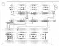
Came home for lunch, checked and fixed the orientation of the IIci Cache Slot connector, flipping my pinouts upside down in the process. :-/   Streched the layout back apart some and then did some doodling at work to illustrate my reasoning for having a daughtercard in the mix. Picked some control lines in a semi random fashion and drew the connections where they run up one side of the header pairs from the PDS to the daughtercard and back down again to the IIci connector on the other row of pins.

I'm limited to 36 to 38 .100 header connections across a 10cm wide SEEED board for prototyping the GAL adaptation. I won't need nearly all the control lines, so between GND and +5V supplied to the daughtercard and a max of 35-37 signals running up one row and back down the other ought to be more than sufficient. All will be a hardwired loopbacks to the main board. Traces will be cut on the daughtercard and patched to the active component(s) inputs as needed. Its outputs will be patched into the appropriate lines wherever they're cut for the output's trip back down to the appropriate pins on the main board.

There are a few address lines involved as well, along with many control lines which can be eliminated. So there'll be a bit of ugly rework to be done on the main board to finally wind up with exactly what is needed heading up to and then back down again from the GAL. Hopefully I can keep rework to a minimum by combing through pinouts of all iterations of passive and active adapters with the help of their owners.

In this manner, ProtoCache3 (in this proposed iteration) remains a constant, or constant after those modifications can be worked out. The plug-in daughtercard prototyping blanks become the equivalent of game cartridges, little expansion cards in their own right for working out successive combination attempts. Plug in circuit boards of an early computer?

 
I hope my explanations about prototyping board development have been clear enough. I'm not so good with getting things across in words, that's why I document progress in pictures. I've been told that doing so helps quite a lot in getting my notions across.

At any rate, here's a better attempt at a summary of events in this thread:

I've been slowly letting go of the notion of wire wrapping the the entire board as I've been ruthlessly applying the KISS principle. I originally wanted to put the GAL prototyping area on the main PCB, but have realized along the way that keeping the main board simple is very important.

Moving the GAL I have in hand to a daughtercard transfers complexity off the oversize/expensive main board while adding flexibility. Adding a DIP socket “in series” with the SMT GAL socket for. testing reproduction versions was in my original spec for the ProtoCach1 wire wrap board. Minimal costs of making up sets of Rpi oriented SEEED boards (used as generic term) has made utilizing them in the daughtercard role a no brainer to me. Such has allowed me to reduce the size of the main board significantly.

I'd worked out a very labor intensive method for using my VinylCAM PCB process to produce a wire wrap oriented board combining soldered connectors with wire wrap headers. I've also got laser print etch mask here, but have never tried it, so I stuck to the tries and true. I decided moving entirely to wire wrap on perf board might be the KISS way to go, built a partial implementation and started this thread.

Themk's cost analysis of various sizes of SEEED boards made me realize that moving back from full-on wire wrap to etched copper would a significant amount of time and effort. A little help and a little over $100 in trade for sweat equity made perfect sense as that decision was made during tax return season. ;)

I'd originally wanted to implement SMT buffering/line driving components for testing more than the two card limited PDS spec. but that fell by the KISS oriented wayside. Board size/cost tradoff pressures have been squeezing my simplified wire wrap header areas coupled to soldered connectors off the board and back onto wire wrap connectors.

I traded the cost of adding another two layers in order to move as much of the wire wrapping of the control line adaptation circuitry onto copper. Per BMOW's suggestions that meandering in wire wrap won't be necessary for the 16MHz SE/30 testbed, I've begun thinking in terms of implementing the 64 Address/Data lines in copper on the ProtoCache board as well. I was thinking that meandering might rear its ugly head on my 25MHz clocked IIsi board, but I'll cross that bridge if and when, might as well burn it for the time being, permanently with luck.

My drilled out via (pre-positioned/single purpose/almost totally unnecessary adjacent triplets per signal) cut and patch process makes moving adaptation oriented addressing rework to short lengths from my now redundant wire wrap spools a snap. Has anyone else used this method? It's one of my normally crazy ideas, but it's hard to image it hasn't occurred to some other lunatic. Such was unnecessary back in the wire wrap day, but things have changed dramatically, so it makes more sense than ever to me in this SEEED age.

At any rate, we're now looking at ready to go ProtoCacheX board development, fully implemented in copper across four layers. The KISS principle eliminates all wire wrap headers to the daughtercard interface at this point. Additional pins will be added as necessary to those drilled out via cutout locations. Wire wrap is far more flexible than directly soldering patch connections during the experimental period. Desoldering the two pins and restoring their drilled out connection with wire wherever jumpering proves unnecessary jibes with the KISS principle in my book.

Dedicated cut and patch provisions for mix and matching traces to the daughtercard pins should keep connections for the adaptation to the 19 lines available (+5V and GND take up the first two) on a single 2x20 header/RA socket interface. Putting the usual suspects on the first 19 pins KIS. Those extra 18 or 19 thru-holes and related signal cutouts provide a comforting level of insurance.

GAH, I really hate writing! What can I do to further clarify this attempts at summation?

Questions?

edit: SWEET!  [:D] ]'>

Here's the link to a similar reboot that does much in explaining the overall project and adaptation development process.

Cloning the Daystar PDS Adapters for the IIsi and SE/30 - Take 2
 
Last edited by a moderator:
Dear Trash,

When the final product is finished will it be one board, like the sketches, or will it be several smaller protoboards offering different connectors?  I wanted to mount two 601 cpu's via cpi's and two pds boards (Radius video, and Asante ethernet) and one nubus.  I know I will probably have to upgrade or replace my PSU.  According to Daystar's marketing material the Turbo 601 was supposed to work in the SE/30 so I'm hoping the 6100's will too, (I 've got several of those).  Will we have a choice in what we order?

Thanks for your time,

TPope

 
Hi TPope,

I'm on vacation, so sorry for the terse reply...

The plan is to have two connectors, with the possibility of three later, after a buffer line driver is designed. For the moment, plan on one IIci cache slot for the accelerator, and one PDS passthrough slot, for video or ethernet. The dream of using all three slot IDs will come later.

Thanks,

mk

 
I hope my explanations about prototyping board development have been clear enough. I'm not so good with getting things across in words, that's why I document progress in pictures. I've been told that doing so helps quite a lot in getting my notions across.
I think I followed most of that. :)

Why is a GAL prototyping area needed at all? Is there some uncertainty as to what the correct mapping of signals should be between the slots?

If some signals are propagated on the main PCB directly between connectors, and others travel from a connector on the main PCB to a daughtercard, to a GAL, out of the GAL, back to the main PCB, to a second connector, then I might be a little worried. That's a different story from a simple difference in trace length of a few cm on a single PCB. My guess is it would still work OK for what you're planning, but it's not ideal. 

You probably know this already, but the power and ground paths between your connectors shouldn't be done with tiny gauge wire-wrap wires. Those will never carry enough current for something like a power-hungry '040 accelerator. The power and GND should be nice fat and wide traces on your main PCB.

Funds and time permitting, my suggestion would be to go straight to a single PCB prototype, and forget about wiring wrapping and prototyping, and just get that thing built asap. Chances are it won't work quite right, or won't work at all, but you can learn from the failures and make a v2 and v3 until you get it right. I personally find this approach better than spending large amounts of time obsessing over making the first version perfect, since it will invariably have flaws anyway.

 
Why is a GAL prototyping area needed at all? Is there some uncertainty as to what the correct mapping of signals should be between the slots?
Big time uncertainty involved across one, two and even three discrete ROMs PALs and GALs on different versions of adapters out there in the field. The two I have on hand are a single GAL implementation for the IIx adapter which I'm hoping will be a silver bullet for the SE/30/IIsi 030 PDS and the three component adaptation of the for the combination of the MacII's O20/MMU sockets. That should be helpful in teasing apart signalling involved between the PowerCache and two individual, stock, well documented parts if it comes to that.

Sorting that mess out is pretty much the heart of this insane quest.

If some signals are propagated on the main PCB directly between connectors, and others travel from a connector on the main PCB to a daughtercard, to a GAL, out of the GAL, back to the main PCB, to a second connector, then I might be a little worried. That's a different story from a simple difference in trace length of a few cm on a single PCB. My guess is it would still work OK for what you're planning, but it's not ideal.
Not what I wanted to hear, but a complication best avoided. Is capacitance introduced by the header connection that's problematic? No clue here, I do electron plumbing, not electronics. I've been contemplating removal of the upper, frog-leap passthru development section for a while. It's now officially KISSed off, all I need is the direct connection wire wrap connector at the bottom of the board. I need it to run a video card while testing passive adaptations on the SE/30 with the Video ROM pulled, putting the kaibosh on any PseudoSlot Video operation memory conflicts in Slot $E induced by cache operations on the accelerator. Hoping to have a IIsi back up and running for the same tests, if and when. The buffered vampire video cutout of the IIsi will definitely free up $E where it's hit or miss for pulling the ROM on the SE/30. I'll add wire wrap provisions for GAL/PAL whatever prototyping to the board where the daughtercard connector resides on that last drawing

You probably know this already, but the power and ground paths between your connectors shouldn't be done with tiny gauge wire-wrap wires. Those will never carry enough current for something like a power-hungry '040 accelerator. The power and GND should be nice fat and wide traces on your main PCB.
Yep, on page two I made the jump from weaving heavy gauge wiring into a wire wrap oriented PCB to weaving the equivalent of Power and Ground planes into fat copper on what was then to ba a two sided PCB.

Funds and time permitting, my suggestion would be to go straight to a single PCB prototype, and forget about wiring wrapping and prototyping, and just get that thing built asap.
Time for futzing is plentiful and enjoyable for me. Funds for boards is another matter entirely. This is puzzle time a fun and games for me, not product development. I've got an expectation level of ZERO for completing this project on my own. I'm just hoping to get enough chickens, ducks and geese arranged any which way I can manage for someone else to say AHA! and then line the proper poultry up in row. :I

 
Last edited by a moderator:
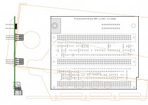
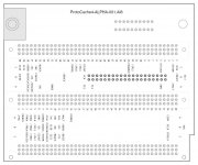
This is Kept about as Simple as it gets. Prototyping area is moved above the Cache Slot to fit in between the mounting lugs. May or not use wire wrap connectors to do modifications in easily reworked wire wrap. Probably so, finding a PLCC socket is going to be interesting, this 20 pin GAL package is square. So far I've only seen rectangular sockets in 20 pin. DIP socket's are easy to find in wire wrap. Dunno, tired, but satisfied I've cut this to the bone and shaved it down to a 10cm x 12cm board.

PC4-Alpha-000.JPG

ProtoCache4-ALPHA-000.PDF


Attachments

Last edited by a moderator:
When the final product is finished will it be one board, like the sketches, or will it be several smaller protoboards offering different connectors?
 
I'm not even thinking in terms of a final product. I just want to get into the puzzle, if I can get outside edges of the problem defined, the pieces in the center may start falling into place.
 
I wanted to mount two 601 cpu's via cpi's and two pds boards (Radius video, and Asante ethernet) and one nubus.  I know I will probably have to upgrade or replace my PSU.  According to Daystar's marketing material the Turbo 601 was supposed to work in the SE/30 so I'm hoping the 6100's will too, (I 've got several of those).
Your notions are more ambitious than mine, that's a compliment. If I can get someone to help out by unraveling the bus mastering foibles peculiar to the SE/30, there may be a chance for fulfilling the NuBus in SE/30 pipe dream. All indications are that the problems lie in that area. Dunno, that's way above my pay grade.

Will we have a choice in what we order?
Not a clue, this isn't a commercial venture, it's supposed to be an open source community development project. Maybe someone will be able to produce and sell adapters at a fair price level. Self-build kits put together by cooperatives might work, dunno. I know I won't be taking any orders. ;)


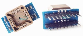
Well, that was easy  .  .  .
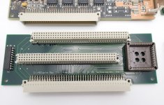
PLCC2DIP-combo.jpg
.  .  .  simplification is on the slow boat at $1.77 per.

The daughtercard's back. I decided your guess that "it would still work OK for what you're planning, but it's not ideal." is plenty good enough for me. Thanks, BMOW! However there's now backup for wire wrapping the implementation directly on the board if necessary. I can also wire the socket up directly after prototyping of the adaptation might be successful. That will eliminate the daughtercard, if and when.

I figure if shields and long jumper wires on breadboards work for prototyping in the world of pi, maybe the daughtercard approach will work for me. It's worth a shot, keeping the ProtoBoard layout a constant is a big deal to me. Using jumpers on the wire wrap pins to make the connections, I can eliminate that silly loopback notion for signal lines not being tested on the daughtercard.

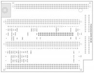
PC$-A-001.JPG

Address and data lines are being moved onto copper traces, so the pinout has been reduced to just the control lines. As they're eliminated I'll remove the fill for that text as well. I figure it's safe to remove the clocks, buslock and NuBus right off the bat? Suggestions for other signals to drop from the suspect list would be greatly appreciated. I'd like to keep the signal chart as clean as possible for the next round of board buzzing.

Time to stop thinking about this for a while, maybe I make some progress. ;)

ProtoCache4-ALPHA-001.PDF


Attachments

Stopped thinking about the ProtoBoard and started thinking about the TwinSlot and DiiMO pinouts. Remembered there's a connection between an address line or two on the passthru connector that might not be connected to the MoBo connector. Which brings me right back to the PCB layout. ::)

Passthru's back and I added a second DIP socket to be wired in series. Using the header pinned adapter will ruin a socket for use with a DIP ICs legs, so the PLCC adapter socket is now tail end Charlie.

PC4-A-100.JPG

DIP socket(s are now consistent with GAL locations on single chip boards. Looking a the pic just now makes me realize I'll have to move the DIP sockets closer to the edge of the board to allow for clearance between the piggybacked PLCC socket and EuroDIN connector. PreVis is everything in movie production these days and one hella tool for me.

ProtoCache4-ALPHA-100.PDF


Attachments

Awesome trash!

I like those PLCC to DIP adaptors, they look very useful!

Here we go!

Some bad news however:

I forgot to put my project files on my USB flash drive that I took with me. Now, that normally wouldn't be a problem, except I was stupid enough to forget to upload it to my NAS. If it was on my NAS I could at least access the files via SFTP, but it's not. Oh well, I should be enjoying vacation, not stressing about projects ;) . I've been purposely limiting my time spent here on the 68kmla, but part of that is due to the fact that touchscreen on-screen keyboards are useless.

 
Last edited by a moderator:
Okay, so I been really busy and off the grid for a while minus the hoarding of new stuff, but I just landed something pretty awesome!

s-l1600.jpg

Now I have to get back into the mix things and help out if you still need it.
 
Absolutely! Could really use some help with that DiiMO board. Any adapter with a single IC implementation is an important piece of the overall puzzle. ATM someone making great progress deciphering the connections on a very similar DayStar DualPort IIsi that he's been running on his SE/30 bench.

He desoldered and socketed the PAL to make things easier, including spelunking its innards eventually. Are you comfortable modifying yours with a socket or sending it to someone adept at the process?

 
The card is arriving later this week with a DiiMO 50mhz card. I will keep you posted as soon as it arrives and take better pix of the pal. I am be open to some possible non-destructive alternation.

 
well, not so quick. if you can see a trace on pin1 and see where it goes, if it isn’t connected to a clock signal, we could still read it out.

A nice clear photo of the back side of that card would be tremendous.

 
Last edited by a moderator:
Back on the DualPort IIsi front, I've finished tracing out all the connections, and have started pulling the equations out of the PAL.

So far:

/* Dedicated input pins */
 
pin 1   = I0; /* Input BGACK  in from CACHE & THRU (held high) */
pin 2   = I1; /* Input R/W in from all slots */
pin 3   = I2; /* Input BG in from PDS30 */
pin 4   = I3; /* Input DS in from all slots */
pin 5   = I4; /* Input RSVD in from PDS30 */
pin 6   = I5; /* Input RESET in from all slots (held high) */
pin 7   = I6; /* Input A0 in from PDS30, THRU, and CACHE slots */
pin 8   = I7; /* Input A1 in from all slots */
pin 9   = I8; /* Input A4 in from all slots */
pin 11  = I9; /* Input CPUDIS in from CACHE (held low) */
 
/* Programmable input/output pins */
 
pin 12  = B0; /* Combinatorial output to BGACK on PDS30 */
pin 13  = B1; /* Combinatorial output to nothing, n.c.*/
pin 14  = B2; /* Combinatorial output to BG on THRU and CACHE slots */
pin 15  = B3; /* Fixed high output to D0 */
pin 16  = B4; /* Fixed high output to D3 */
pin 17  = B5; /* unknown */
pin 18  = B6; /* unknown */
pin 19  = B7; /* Fixed high output to nothing, n.c. */
 
/* Output equations */
 
 B7 = 'b'1;
 B4 = 'b'1;
 B3 = 'b'1;
!B2 = !I2 & !I9;
!B1 = !I6 & !I7 & !I8;
 B0 =  I0 & !I9;
 
I'm still working on B5 and B6.  Seems as though the input/output state of those pins are controlled by one of the other outputs, I'm guessing B1 since its output isn't connected to anything on the adapter card. Its state must be used for something, otherwise why have an equation assigned to it?
 
Back
Top