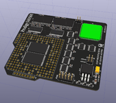
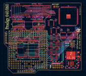
New Project: Prodigy 040/060 Card

Hello Mac community,

I joined MLA68K 2 days ago, because I recently acquired a Macintosh LC475, which I have started to like a lot due to its compact size, and actually very good performance.

Most people know me in the Amiga community, where I have started several hardware designs ranging from sound card, graphics card and cpu accelerators.

So by using Shapeshifter since almost 30 years, one could call me a "passive Mac user", since I have gotten to really like the Mac OS itself, but also the vast choice of native 68k software I could suddenly use on my Amiga at great speed. ;)

I have recently stumbled across the great efforts made by @zigzagjoe to get a 68060 CPU running in a real MAC, something that Amiga users have been doing since a long time, and sadly never passed back to the MAC community due to the emergence of PPC-based machines.

The most prominent headline of this effort, which actually sparked my interest here, was "The Fastest (68k) Macintosh Might Not Be An Amiga Anymore". So I asked myself: well, why not give something back, and make this a reality. Because, at least that's my perspective, what unites both our communities is the love and passion for the Motorola 68k CPU architecture, which, still to this day, is amongst the best, if not the best, CISC ISA ever been created.
:)

(Some people might even claim it should never have been superseded by PPC..... ;))

As a lucky coincidence, I have recently started to make my own Amiga 68060-based accelerator design a while back, which I am waiting now for the very first Revision 0 prototype PCB. Lucky, because I can actually re-use most of my design for a classic m68k MAC accelerator. Therefore, as my introduction to this community, I would proudly like to annouce the:

Prodigy 040/060 Card

So what is this card? In short, it is a CPU card for classic 68k-based MACs, which plugs directly into the 68040 CPU Socket.

Here is a rendering of the first prototype:
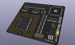
Screenshot 2026-01-02 220932.png

The card will have the following features:
  • Support for 68040 and 68060 CPUs, selectable by jumper setting.
  • CPU clock rate: up to 50MHz (68040) and, yes, 100MHz! (68060)
  • SDRAM memory controller, which runs at either 1x or 2x bus speed (to minimize first access penalty) - meaning up to 100MHz memory clock
  • 128MB on-board SDRAM
  • Flexible bus interface: always full speed to SDRAM, selectable 1/2 or 1/4 bus speed to MAC mainboard (no need to overclock SCSI bus in order to run 100MHz!)
  • 2 MB Flash Rom, for startup code, 68060 compatibility software layer and patching of MAC OS
  • RECOVERY jumper: if set, system starts using the mainboard ram and rom, enabling you to flash the rom via software
  • A prominent Amiga feature: MAPROM - copy the MacOS Rom to superfast SDRAM on start-up, and use memory protection/remapping to execute it as if it were a real ROM - withou the need of using the MMU
  • Configuration settings can be flashed in FPGA
  • FPGA can be software upgraded on the MAC
  • Designed to (hopefully) fit in all 68k-based MACs, first prototype will be developed on an LC475
This card will bring significant acceleration even if you keep using your on-board 68040 CPU due to its superior memory interface.

So, what do you think? ;-)

What I would like to ask you is, whether you think this product might be useful to you, and if yes, since I am basically "an Amiga guy", I would appreciate if you could guide me a bit on how these features could be implemented the best way in software to integrate well with MacOS.

So for example, I can design a memory controller very easily, but I have currently no idea how I can make this memory available to MAC OS in the most system friendly way. On Amiga, this is actually quite easy, since the Amiga implements a card resource management system called "Autoconfig", making it very easy to make the OS recognize additional memory and I/O resources (much like PCI).

From what I have gathered so far, the way to go here would be to patch the MacOS Rom to utilize the new resources without getting into conflict with the on-board hardware.

In any case, I shall be looking forward to your feedback and help! :-)

Best regards,

Oliver Achten
 
Last edited:
Hello Mac community,

I joined MLA68K 2 days ago, because I recently acquired a Macintosh LC475, which I have started to like a lot due to its compact size, and actually very good performance.

Most people know me in the Amiga community, where I have started several hardware designs ranging from sound card, graphics card and cpu accelerators.

So by using Shapeshifter since almost 30 years, one could call me a "passive Mac user", since I have gotten to really like the Mac OS itself, but also the vast choice of native 68k software I could suddenly use on my Amiga at great speed. ;)

I have recently stumbled across the great efforts made by @zigzagjoe to get a 68060 CPU running in a real MAC, something that Amiga users have been doing since a long time, and sadly never passed back to the MAC community due to the emergence of PPC-based machines.

The most prominent headline of this effort, which actually sparked my interest here, was "The Fastest (68k) Macintosh Might Not Be An Amiga Anymore". So I asked myself: well, why not give something back, and make this a reality. Because, at least that's my perspective, what unites both our communities is the love and passion for the Motorola 68k CPU architecture, which, still to this day, is amongst the best, if not the best, CISC ISA ever been created.
:)

(Some people might even claim it should never have been superseded by PPC..... ;))

As a lucky coincidence, I have recently started to make my own Amiga 68060-based accelerator design a while back, which I am waiting now for the very first Revision 0 prototype PCB. Lucky, because I can actually re-use most of my design for a classic m68k MAC accelerator. Therefore, as my introduction to this community, I would proudly like to annouce the:

Prodigy 040/060 Card

So what is this card? In short, it is a CPU card for classic 68k-based MACs, which plugs directly into the 68040 CPU Socket.

Here is a rendering of the first prototype:

View attachment 93907

The card will have the following features:
  • Support for 68040 and 68060 CPUs, selectable by jumper setting.
  • CPU clock rate: up to 50MHz (68040) and, yes, 100MHz! (68060)
  • SDRAM memory controller, which runs at either 1x or 2x bus speed (to minimize first access penalty) - meaning up to 100MHz memory clock
  • 128MB on-board SDRAM
  • Flexible bus interface: always full speed to SDRAM, selectable 1/2 or 1/4 bus speed to MAC mainboard (no need to overclock SCSI bus in order to run 100MHz!)
  • 2 MB Flash Rom, for startup code, 68060 compatibility software layer and patching of MAC OS
  • RECOVERY jumper: if set, system starts using the mainboard ram and rom, enabling you to flash the rom via software
  • A prominent Amiga feature: MAPROM - copy the MacOS Rom to superfast SDRAM on start-up, and use memory protection/remapping to execute it as if it were a real ROM - withou the need of using the MMU
  • Configuration settings can be flashed in FPGA
  • FPGA can be software upgraded on the MAC
  • Designed to (hopefully) fit in all 68k-based MACs, first prototype will be developed on an LC475
This card will bring significant acceleration even if you keep using your on-board 68040 CPU due to its superior memory interface.

So, what do you think? ;-)

What I would like to ask you is, whether you think this product might be useful to you, and if yes, since I am basically "an Amiga guy", I would appreciate if you could guide me a bit on how these features could be implemented the best way in software to integrate well with MacOS.

So for example, I can design a memory controller very easily, but I have currently no idea how I can make this memory available to MAC OS in the most system friendly way. On Amiga, this is actually quite easy, since the Amiga implements a card resource management system called "Autoconfig", making it very easy to make the OS recognize additional memory and I/O resources (much like PCI).

From what I have gathered so far, the way to go here would be to patch the MacOS Rom to utilize the new resources without getting into conflict with the on-board hardware.

In any case, I shall be looking forward to your feedback and help! :-)

Best regards,

Oliver Achten
Great to have more hardware developers in the community!

Overall I think you'll find the Mac ROM is much, much less auto-configurable (more like Kickstart 1.x than 2.x+). Using your memory example:
  • ROMs are "universal", but only in theory. Despite many machines shipping with ROM SIMM slots, upgrades were never provided and compatibility was never really ensured. So while the ROM itself supports earlier machines, it was never debugged for regressions. As a result, some ROMs can be used across machines (IIsi -> SE/30, LC 475 -> Wombat-based Quadra), but not always, and there's often quirks (LC 475 ROMs have the wrong memory timing for instance).
  • Most machines have different ROMs (though there's some overlap), meaning offsets are different per machine.
  • The ROMs do autodetect the logic board type using resistor matrices, etc, and configure themselves accordingly.
  • Combining this, let's look at memory sizing, which I happened to be debugging yesterday:
    • The ROM detects what machine it's running on.
    • It branches to the correct memory sizing routine for the memory controller corresponding to that machine.
    • It builds a table of memory chunks in memory.
    • It returns a pointer to that table for configuration of the rest of the system.
So this might not be too bad in theory, you can patch in your own memory controller routine and jump to it to add those address ranges. But there's a few challenges to think about:
  • You need to choose a single ROM and set of machines to support, or build a table of patches per ROM.
  • It's possible the OS overpatches these routines itself (unlikely for memory sizing, but common for other routines) which you need to avoid or re-patch.
  • It's possible other parts of the ROM or OS size memory on their own; since it wasn't meant to be extended, these quirks may not have been discovered yet by the community.
Despite this, it's definitely doable. The Turbo040 does a large amount of patches for a large amount of ROMs to enable 040 compatibility on 030 machines, for instance. Overall I'd look at targeting the LC 475 ROM, as it has the widest '040 machine support (with a few fix-ups).

For mapping ROM to RAM, here's a relevant discussion on a software utility (w/ benchmarks and more): https://68kmla.org/bb/threads/rom-in-ram-for-quadra-performance-boost.46536/

Were you planning for software configurable clock speeds?

As a real challenge, A/UX support would be very interesting, since it never ran beyond 68k. I'm not sure how it handles 040 compatibility (It mostly doesn't use the ROM, so I'm not sure where its support packages come from -- it might depend on the normal OS boot gluing everything together).
 
This sounds great! I have a few Amigas with (your???) accelerators, including the ACA500, ACA1234 (with an FPU upgrade), as well as the AGA MK3.

As the previous poster, I'm also curious how this will work across different models. AFAIK, there's a lot of proprietary trickery that was implemented on the old-school accelerators. Also, there are many different board layouts and while some accelerators worked on multiple "sibling" models, they had to use a variety of adapters to make it work.

Oh, one other thought. I'm wondering how "useful" (LOL) a 100MHz 68060 would be on a Mac. There just wasn't a lot of 68k Mac software written that would need that much speed. Later software was written for the PPC, so there's sort of a cut-off to where speed gains just outpace any software ever written for the platform. It's quite different than the Amiga scene where people are creating demos to this day. :)

Regardless, it's quite an exciting prospect and I'm sure there would be many people interested in the product.

Following this with great interest.
 
Last edited:
Oh, one other thought. I'm wondering how "useful" (LOL) a 100MHz 68060 would be on a Mac. There just wasn't a lot of 68k Mac software written that would need that much speed. Later software was written for the PPC, so there's sort of a cut-off to where speed gains just outpace any software ever written for the platform. It's quite different than the Amiga scene where people are creating demos to this day. :)
You'd be surprised. So much was still emulated on PowerPC, and it was "fast enough" that applications took awhile to transition.

In the same vein, obviously running System 7 on a New World G4 will smoke any '060 anyway, but that's no fun (well it is fun, but differently fun).

That said, I think slow graphics and anemic disk performance will indeed drag down the overall "experience" to make it less impressive than on an Amiga. With graphics running at standard clocks on the 040 bus (or NuBus) and 5MB/s SCSI, I suspect things like Finder won't feel a lot faster.

But any period productivity app should fly, I would think.
 
Hi everyone,

Overall I think you'll find the Mac ROM is much, much less auto-configurable (more like Kickstart 1.x than 2.x+). Using your memory example:

that's what I sort of expected after doing some initial research. I mean, coming originally from the C64, I'm not that unfamiliar in getting "my hands dirty" in delving into low-level bootstrap code, which sort of has an underlying structure, but was never documented or defined in a way to provide standardised interfaces. But I suppose, that's also the fun and challenge here. ;-)

So this might not be too bad in theory, you can patch in your own memory controller routine and jump to it to add those address ranges. But there's a few challenges to think about:
  • You need to choose a single ROM and set of machines to support, or build a table of patches per ROM.
  • It's possible the OS overpatches these routines itself (unlikely for memory sizing, but common for other routines) which you need to avoid or re-patch.
  • It's possible other parts of the ROM or OS size memory on their own; since it wasn't meant to be extended, these quirks may not have been discovered yet by the community.

I was actually thinking about applying patches to the ROM after my initial boot code has copied it to RAM. With the consequence that, for all known and documented ROMs, there are tables which contain the location offsets for each routine that needs to be patched.

The memory controller might perhaps not be the biggest challenge, as I expect that this can be resolved by replacing the memory init routine altogether, but adding the support code for the 68060, including the emulation layer for the unsupported opcodes.

Can you guys recommend me any source on how to get an overview, does a so-called "ROM Kernel Reference" exist for the Macintosh?

For mapping ROM to RAM, here's a relevant discussion on a software utility (w/ benchmarks and more): https://68kmla.org/bb/threads/rom-in-ram-for-quadra-performance-boost.46536/

Thanks, I'll have a look into this. My plan is to implement the memory remapper in the FPGA, so that the Ram-based Rom layer sits "on-top" of the original physical address space.
https://68kmla.org/bb/threads/rom-in-ram-for-quadra-performance-boost.46536/
Were you planning for software configurable clock speeds?

My plan is to go with the BUS clock provided by the motherboard, and use the PLL in the FPGA to generate the Processor Clock and memory clock.

So depending on the CPU, for example, I can have:

25MHz bus clock (provided by mainboard)
50MHz CPU clock (generated by PLL) -> can be used as PCLK and /or BCLK for the on-board memory controller
100MHz memory clock (generated by PLL) -> can be used as PCLK and / or BCLK (060) for the on-board memory controller.

With the clock obviously changing, as per setting of the mainboard PLL.

The initial boot rom code will detect the CPU type, and adjust the settings according to the values provided in the FPGA flash rom.

As a real challenge, A/UX support would be very interesting, since it never ran beyond 68k. I'm not sure how it handles 040 compatibility (It mostly doesn't use the ROM, so I'm not sure where its support packages come from -- it might depend on the normal OS boot gluing everything together).

You mean UNIX? Yes, that definetely would be a great challenge, perhaps even providing the boot loader inside the ROM of the card. :-)

Thanks for your warm welcome and help! :-)
 
Oh, one other thought. I'm wondering how "useful" (LOL) a 100MHz 68060 would be on a Mac. There just wasn't a lot of 68k Mac software written that would need that much speed. Later software was written for the PPC, so there's sort of a cut-off to where speed gains just outpace any software ever written for the platform. It's quite different than the Amiga scene where people are creating demos to this day.
It would enable us to write more software - newer audio codecs, SSH and SSL working better, games like Marathon, Dark Forces, Doom and Quake, that there are 68k version of, would run better...

We're not limited to existing software.

Even then, Photoshop, Illustrator, ProTools... Premiere... Infini-D Etc... All benefit from better drawing / rendering times.
 
That said, I think slow graphics and anemic disk performance will indeed drag down the overall "experience" to make it less impressive than on an Amiga. With graphics running at standard clocks on the 040 bus (or NuBus) and 5MB/s SCSI, I suspect things like Finder won't feel a lot faster.
Nothing really stopping us aiming for a 50MHz bus on the LC 475 :)

20251228_224226.jpg
 
The memory controller might perhaps not be the biggest challenge, as I expect that this can be resolved by replacing the memory init routine altogether, but adding the support code for the 68060, including the emulation layer for the unsupported opcodes.
Just to keep in mind, the stock Memory Controller will likely still need some initialisation as it is also an integral part of other systems like graphics. (It generates and controls video clocks like pixel clock, hsync, vsync etc).

Can you guys recommend me any source on how to get an overview, does a so-called "ROM Kernel Reference" exist for the Macintosh?
If you aren't aware of this, this is leaked ROM source for the 840av ROM. It is from a similar era to the 475. There are also tools the community has made for the analysis of ROM binaries... But I'm not familiar with them so will leave others to discuss.


With the clock obviously changing, as per setting of the mainboard PLL.
I assume you're aware, the bus speed can be set dynamically on the LC 475. This is super unusual and the only 68k desktop Mac that we are aware it is possible for. On a stock machine they're mostly stable up to 33MHz at which point you have to move a resistor to divide the clock to the SCSI chip by two (some people have trouble even at 33MHz), then they boost to about 40 to 43MHz before they reach the limit of a MC88920 PLL... If you swap in an MC88916DW80, the CPU grade becomes the limit up to about 52MHz. I haven't invested the cause of that limit, not sure if it is CPU, ROM, RAM, VRAM or chipset. Or even board.
 
Last edited:
I didn't see this thread so I replied to your posts in my 68060 redux thread first... quoted below.

The MMU is mostly used for 24/32 bit mode, cache management, and one or two machines to make memory contiguous or handle framebuffer in DRAM. The MEMC (650/800) is foundational to the system so initialization can't be skipped. Same for the other 040-class machines. You would need to step in somewhere in the sizemem process after it's initialized. Not impossible, but a complication.

I would however gently suggest that you may want to slow roll the hardware in favor of working the 060-centric software challenges first that I've laid out in this thread. Solvable issues, I think, with some difficulty, but I'd recommend tackling those first as otherwise you may end up with some nice hardware that can't be used. Not trying to tell you how to work your projects or implying that's what will happen here :) but from experience it's been a reoccurring pattern (myself included) where it's "easy" to build some hardware but the software side never happens as it turns out more difficult than anticipated.

What trips folks up is the relatively complex (and ill-documented) software environment and monolithic ROM / OS design. I'm still particularly concerned about the vector table being manipulated by "user" and OS code. If you have some interest in working on the ROM you may want build one of my ISP-SIMM as it supports loading ROM code via USB to an installed ROM module for quicker iteration. It was foundational to the work I did getting the IPSP/FPSP and other ROM modifications developed for this as well as other development work.

On the hardware: you should be able to quiesce the built in RAM controller by pulling on /MI at the appropriate times, but keep in mind these systems do use DMA at least for onboard ethernet and often nubus so DMA / bus arbitration must be appropriately handled by your logic on the card. I've been idly curious if an 060 would have a fit if you set up a 1/3 multiplier, while it's not explicitly supported, I think there's a chance it may work. For a "simple" 040 to 060 adapter that'd provide the best-case as you could pretty easily get max performance out of the CPU while not crippling DRAM/VRAM/ROM accesss as badly.

Onboard DRAM would help 060s but it's less essential as the memory situation on the 68040 macs is far less dire than Amiga with the native 040 bus and performant memory controller supporting bursts/interleave. For a drop in 060 accelerator built-in ROMs as you did would be best as the ROM slots are not typically populated in 040 macs, but you'll have difficulty in that these machines are unable to boot an 060 without modified ROMs. ROM in RAM is not a bad thing to have either - it's been implemented in a few vintage designs. It provides some benefit though it's not mandatory as the hottest ROM routines fit in the 040 caches.

Attached are a number of relevant datasheets/schematics you might find interesting. In my github repository a number of useful software sources are linked including the supermario dump which contains a significant amount of ROM code from the end of the 68K machines (840av).
 

Attachments

Just to keep in mind, the stock Memory Controller will likely still need some initialisation as it is also an integral part of other systems like graphics. (It generates and controls video clocks like pixel clock, hsync, vsync etc).

Thanks, @zigzagjoe has provided to me the necessary datasheets, so I can have a better overview how the functions are related to each other. I assume that the ROM also defines which video modes are available based on the state of the mode pins of the video connector, correct? (much like a VGA/VESA bios rom?)

If you aren't aware of this, this is leaked ROM source for the 840av ROM. It is from a similar era to the 475. There are also tools the community has made for the analysis of ROM binaries... But I'm not familiar with them so will leave others to discuss.


Thanks, that'll give me a great starting point! :-)

I assume you're aware, the bus speed can be set dynamically on the LC 475. This is super unusual and the only 68k desktop Mac that we are aware it is possible for. On a stock machine they're mostly stable up to 33MHz at which point you have to move a resistor to divide the clock to the SCSI chip by two (some people have trouble even at 33MHz), then they boost to about 40 to 43MHz before they reach the limit of a MC88920 PLL... If you swap in an MC88916DW80, the CPU grade becomes the limit up to about 52MHz. I haven't invested the cause of that limit, not sure if it is CPU, ROM, RAM, VRAM or chipset. Or even board.

As I said, my plan is that I always run the CPU synchronously to the BUS clock of the MAC. In the FPGA itself, I will use the bus clock then to feed its own PLL to generate all subsequent internal clocks.

Which means that, changing the bus clock itself will also change the clock of the CPU and memory. But, on top of that, I can now decide in software whether the CPU PCLK or Memory runs now at 2x, 3x or 4x the bus clock. Accesses to the SDRAM will always use the fastest bus clock option available for the given CPU, while keeping accesses to the mainboard synchronous.

I didn't see this thread so I replied to your posts in my 68060 redux thread first... quoted below.

Yeah, sorry for having "hijacked" your thread, but on the other hand, your effort basically gave me now the motivation to do this accelerator design, based on my original effort for the Amiga. :-)

The MMU is mostly used for 24/32 bit mode, cache management, and one or two machines to make memory contiguous or handle framebuffer in DRAM. The MEMC (650/800) is foundational to the system so initialization can't be skipped. Same for the other 040-class machines. You would need to step in somewhere in the sizemem process after it's initialized. Not impossible, but a complication.

My intention is that everything related to remapping resources during the low-level initialisation is handled by the FPGA. So you can select different physical memory address layouts based on the requirements of the machine, and actual boot process.

I would however gently suggest that you may want to slow roll the hardware in favor of working the 060-centric software challenges first that I've laid out in this thread. Solvable issues, I think, with some difficulty, but I'd recommend tackling those first as otherwise you may end up with some nice hardware that can't be used.

Well, that's why my hardware is designed for both 040 and 060. An 040 already strongly benefits from a high-speed memory interface in "everyday world" application. Its only downside to the 060 is actually, really, mostly the FPU, and the inability to achieve even higher clock speeds, which the last revision of the 060 can handle without issues.

Not trying to tell you how to work your projects or implying that's what will happen here :) but from experience it's been a reoccurring pattern (myself included) where it's "easy" to build some hardware but the software side never happens as it turns out more difficult than anticipated.

But that's a general matter of how oneself keeps motivated. As I said, there is a huge overlap in design effort with my Amiga accelerator, so designing the hardware basically comes "for free". As a starting point, the first thing I will do is to plug in a nice L88M 68040 in my accelerator, and going step-by step.

The good thing about using an FPGA for such a design is that I can instantiate a logic analyzer, and basically can trace every single bus access the CPU is doing. So I can specifically trigger on individual accesses to memory and registers, debugging both code and hardware simultaneously.

What trips folks up is the relatively complex (and ill-documented) software environment and monolithic ROM / OS design. I'm still particularly concerned about the vector table being manipulated by "user" and OS code. If you have some interest in working on the ROM you may want build one of my ISP-SIMM as it supports loading ROM code via USB to an installed ROM module for quicker iteration. It was foundational to the work I did getting the IPSP/FPSP and other ROM modifications developed for this as well as other development work.

Thanks, what I am going to start with is, firstly, to get the CPU running, and subsequently bring each function "step by step" to life, firstly on a base of using the rom of my LC475.

The first function I am going to implement is flashing the on-board memory, and then starting to write a small "low level" startup code, which firstly sets-up the accelerator, checks the CPU and machine configuration, copies the ROM to RAM, and then applying patches depending on the makeup of the system, write protecting the mapped ROM, and then kicks-off the cold-/warmstart procedure.

Something doesn't go well? Then just set the "RECOVERY" jumper on the PCB, which disables most of the accelerator functions, except the access to the Flash-Rom, mapped at a different location so it can be reflashed/written.

And I think this would go very well hand-in hand with your substantial work on the 68060 CPU integration. If you like, I could send you one prototype at some point once I can confirm that the hardware is working on the 040.

The good thing is also that you can completely reprogram the FPGA from the MAC host system - I have implemented the same feature on my Amiga projects.

On the hardware: you should be able to quiesce the built in RAM controller by pulling on /MI at the appropriate times, but keep in mind these systems do use DMA at least for onboard ethernet and often nubus so DMA / bus arbitration must be appropriately handled by your logic on the card.

This is a very good point you are addressing - can I actually snoop DMA transactions from the 68040 socket? On the LC475, it seems that "PRIMETIME" is handling the legacy 68030 bus for the PDS slot and also connects to the 53C96 SCSI chip -> would "PRIMETIME" be responsible to take the 040 "off the bus" and act as a 040 bus master towards MEMC(JR) during DMA?

The problem would be that I very well could catch data being written, but not provide data on my own due to potential bus contention when MEMC(Jr) answers a DMA read request. I still need to understand if and how DMA is used in each MAC model, starting from my own LC475. ;-)

I've been idly curious if an 060 would have a fit if you set up a 1/3 multiplier, while it's not explicitly supported, I think there's a chance it may work. For a "simple" 040 to 060 adapter that'd provide the best-case as you could pretty easily get max performance out of the CPU while not crippling DRAM/VRAM/ROM accesss as badly.

I think it depends on how you treat the assertion of the "_CLKEN" signal in relation to both clock domains. On an FPGA, you can, say, time such kind of logic in a synchronous manner by running the logic at a much higher speed.

Onboard DRAM would help 060s but it's less essential as the memory situation on the 68040 macs is far less dire than Amiga with the native 040 bus and performant memory controller supporting bursts/interleave.

I suppose yes, but nevertheless, a 40MHz 040 can push more than 65MB/s using a SDRAM controller design, which minimizes "first access penalty" by running the memory at, say, PCLK speed (80MHz), not BCLK. In this scenario, the 040 actually comes pretty close to the 060 in typical application-related scenarios, and might even surpass it.

The 060 design starts to really pay off in FPU-heavy workloads, and , due to the process technology, running it at actual 100MHz PCLK & BCLK.

For a drop in 060 accelerator built-in ROMs as you did would be best as the ROM slots are not typically populated in 040 macs, but you'll have difficulty in that these machines are unable to boot an 060 without modified ROMs.
Yes, as long as there are no 060 roms, most of the development hast to start on the 040. I could imagine that a small bootloader could run from the roms, which allows to directly load / manipulate memory via a serial interface terminal, so you can have relatively fast "turn-around-cycles".

ROM in RAM is not a bad thing to have either - it's been implemented in a few vintage designs. It provides some benefit though it's not mandatory as the hottest ROM routines fit in the 040 caches.

Usually, ROM-based disk drivers heavily profit from being run from RAM, but maybe that's already happening here.

Attached are a number of relevant datasheets/schematics you might find interesting. In my github repository a number of useful software sources are linked including the supermario dump which contains a significant amount of ROM code from the end of the 68K machines (840av).

WOW! Thanks a lot, for sure I'll have some reading material now for the next days! :-)

Again, I personally see this as a challenge, and an opportunity to get more "acquainted" with the classic Mac community. :-)
 
Last edited:
This is a very good point you are addressing - can I actually snoop DMA transaction from the 68040 socket? On the LC475, it seems that "PRIMETIME" is handling the legacy 68030 bus for the PDS slot and also connects to the 53C96 SCSI chip -> would "PRIMETIME" be responsible to take the 040 "off the bus" and act as a 040 bus master towards MEMC(JR) during DMA?
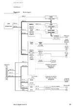
Bit of a high level overview of the 475. From the Dev note :


1000033191.jpg
 
Thanks, @zigzagjoe has provided to me the necessary datasheets, so I can have a better overview how the functions are related to each other. I assume that the ROM also defines which video modes are available based on the state of the mode pins of the video connector, correct? (much like a VGA/VESA bios rom?)


Thanks, that'll give me a great starting point! :-)


As I said, my plan is that I always run the CPU synchronously to the BUS clock of the MAC. In the FPGA itself, I will use the bus clock then to feed its own PLL to generate all subsequent internal clocks.

Which means that, changing the bus clock itself will also change the clock of the CPU and memory. But, on top of that, I can now decide in software whether the CPU PCLK or Memory runs now at 2x, 3x or 4x the bus clock. Accesses to the SDRAM will always use the fastest bus clock option available for the given CPU, while keeping accesses to the mainboard synchronous.


Yeah, sorry for having "hijacked" your thread, but on the other hand, your effort basically gave me now the motivation to do this accelerator design, based on my original effort for the Amiga. :-)


My intention is that everything related to remapping resources during the low-level initialisation is handled by the FPGA. So you can select different physical memory address layouts based on the requirements of the machine, and actual boot process.


Well, that's why my hardware is designed for both 040 and 060. An 040 already strongly benefits from a high-speed memory interface in "everyday world" application. Its only downside to the 060 is actually, really, mostly the FPU, and the inability to achieve even higher clock speeds, which the last revision of the 060 can handle without issues.


But that's a general matter of how oneself keeps motivated. As I said, there is a huge overlap in design effort with my Amiga accelerator, so designing the hardware basically comes "for free". As a starting point, the first thing I will do is to plug in a nice L88M 68040 in my accelerator, and going step-by step.

The good thing about using an FPGA for such a design is that I can instantiate a logic analyzer, and basically can trace every single bus access the CPU is doing. So I can specifically trigger on individual accesses to memory and registers, debugging both code and hardware simultaneously.


Thanks, what I am going to start with is, firstly, to get the CPU running, and subsequently bring each function "step by step" to life, firstly on a base of using the rom of my LC475.

The first function I am going to implement is flashing the on-board memory, and then starting to write a small "low level" startup code, which firstly sets-up the accelerator, checks the CPU and machine configuration, copies the ROM to RAM, and then applying patches depending on the makeup of the system, write protecting the mapped ROM, and then kicks-off the cold-/warmstart procedure.

Something doesn't go well? Then just set the "RECOVERY" jumper on the PCB, which disables most of the accelerator functions, except the access to the Flash-Rom, mapped at a different location so it can be reflashed/written.

And I think this would go very well hand-in hand with your substantial work on the 68060 CPU integration. If you like, I could send you one prototype at some point once I can confirm that the hardware is working on the 040.

The good thing is also that you can completely reprogram the FPGA from the MAC host system - I have implemented the same feature on my Amiga projects.


This is a very good point you are addressing - can I actually snoop DMA transactions from the 68040 socket? On the LC475, it seems that "PRIMETIME" is handling the legacy 68030 bus for the PDS slot and also connects to the 53C96 SCSI chip -> would "PRIMETIME" be responsible to take the 040 "off the bus" and act as a 040 bus master towards MEMC(JR) during DMA?

The problem would be that I very well could catch data being written, but not provide data on my own due to potential bus contention when MEMC(Jr) answers a DMA read request. I still need to understand if and how DMA is used in each MAC model, starting from my own LC475. ;-)


I think it depends on how you treat the assertion of the "_CLKEN" signal in relation to both clock domains. On an FPGA, you can, say, time such kind of logic in a synchronous manner by running the logic at a much higher speed.


I suppose yes, but nevertheless, a 40MHz 040 can push more than 65MB/s using a SDRAM controller design, which minimizes "first access penalty" by running the memory at, say, PCLK speed (80MHz), not BCLK. In this scenario, the 040 actually comes pretty close to the 060 in typical application-related scenarios, and might even surpass it.

The 060 design starts to really pay off in FPU-heavy workloads, and , due to the process technology, running it at actual 100MHz PCLK & BCLK.


Yes, as long as there are no 060 roms, most of the development hast to start on the 040. I could imagine that a small bootloader could run from the roms, which allows to directly load / manipulate memory via a serial interface terminal, so you can have relatively fast "turn-around-cycles".


Usually, ROM-based disk drivers heavily profit from being run from RAM, but maybe that's already happening here.


WOW! Thanks a lot, for sure I'll have some reading material now for the next days! :-)

Again, I personally see this as a challenge, and an opportunity to get more "acquainted" with the classic Mac community. :-)

At least on the 475 DMA is "public" in that the 040 will see /TA and /TS while a device on the LC PDS slot conducts DMA transfers. Nothing else on a 475 will do DMA. On other machines the SONIC will do DMA but the SCSI controller ironically despite being DMA capable is only used in a "psuedo-DMA" mode which the CPU is responsible for the data transfer. Nubus cards would be the bigger concern. Even as apple didn't actually use the snooping mode of the 040 and they appear to have designed for the possibility of using it so that eases things somewhat. The bus arbitration as you're likely aware happens in the chipset not the CPU so that may present some interesting problems but I think as long as you decode for RAM accesses and pull on /MI it should allow your memory controller to reply instead. Of course, you now have to arbitrate the memory access between the CPU and rest of system, but this is rare enough that it shouldn't be the end of the world. DMA is fairly uncommon on Macs.

Are you talking something tighter than 2-1-1-1 memory timings on the 040? I was able to achieve what ought to be 3-1-1-1 operation out of the onboard DRAM controller at 40mhz, so that's where the assertion accelerator-local DRAM is somewhat less relevant comes from. I spent a bit of time developing a prototype next accelerator designed for 25mhz system bus / 50mhz accelerator bus + cache clock / 100mhz pclk and did a bit of exploration around timings then. I was able to get the 040 up to 57mhz bclk before things started getting too loose.

Disk drivers run from RAM, yes, though SCSI manager code (low level stuff) may or may not depending if the OS has patched it. Good point about a monitor though, it's not hard to bring up the serial ports - code is in the repo for that - though speed isn't great. Main problem that i continue to struggle with from a code perspective is a "maintainable" way to handle those binary patches, the best I came up with was binary to -> ASM with labels from the supplied mapping files, then by hand replacing portions from disassembly/supermario as needed.... not great.
 
At least on the 475 DMA is "public" in that the 040 will see /TA and /TS while a device on the LC PDS slot conducts DMA transfers. Nothing else on a 475 will do DMA.

That's good to know. But I can actually support DMA transfers, given that no other slave on the bus will attempt to terminate/acknowledge the bus cycle.

On other machines the SONIC will do DMA but the SCSI controller ironically despite being DMA capable is only used in a "psuedo-DMA" mode which the CPU is responsible for the data transfer.

Interesting, because the schematics of the LC475 would imply that the NCR can do DMA via Prime Time. On the Amiga 3000, SCSI does support DMA, and yes, it is a pain to support it for a CPU accelerator card. ;-)

Nubus cards would be the bigger concern. Even as apple didn't actually use the snooping mode of the 040 and they appear to have designed for the possibility of using it so that eases things somewhat. The bus arbitration as you're likely aware happens in the chipset not the CPU so that may present some interesting problems but I think as long as you decode for RAM accesses and pull on /MI it should allow your memory controller to reply instead.

From which location can I assert /MI? It seems only available directly at the chip.

Of course, you now have to arbitrate the memory access between the CPU and rest of system, but this is rare enough that it shouldn't be the end of the world. DMA is fairly uncommon on Macs.

I think it mostly concerns the question in which regions I could map the SDRAM without interference from another memory slave. I already made the design in a way so that the FPGA recognizes when the 040/060 is not bus master anymore, and can respond to requests from another DMA host (which, I assume, is PRIMETIME in the case of the LC475).

So I probably have to abandon the idea of placing the SDRAM in the same memory space as MEMCJR would map. But what happens if another DMA master writes to, e.g. 0x60000000-0x8ffffffff or 0xa0000000-0xefffffff ? Is this transfer still acknowledged by MEMC(JR)? Or can I acknowledge the Transfer in this space using my own timing?

And another concern is, how to handle the 68000 vector space from physical address 0x0-0xfff?

Are you talking something tighter than 2-1-1-1 memory timings on the 040?

I think 1-1-1-1 can be supported, if the DRAM controller will apply a prefetching strategy. Otherwise, 2-1-1-1 will apply here.

I was able to achieve what ought to be 3-1-1-1 operation out of the onboard DRAM controller at 40mhz, so that's where the assertion accelerator-local DRAM is somewhat less relevant comes from.

Even on a single non-interleaved memory bank scenario such as on the LC475? I don't think this is possible with standard 60ns DRAM. Most designs usually opt for a 3-2-2-2 or even worse timing in this case.

I spent a bit of time developing a prototype next accelerator designed for 25mhz system bus / 50mhz accelerator bus + cache clock / 100mhz pclk and did a bit of exploration around timings then. I was able to get the 040 up to 57mhz bclk before things started getting too loose.

By using a L2 cache with fast SRAM?

Disk drivers run from RAM, yes, though SCSI manager code (low level stuff) may or may not depending if the OS has patched it.

We'll see, I'm going to implement it in any case. ;-)

Good point about a monitor though, it's not hard to bring up the serial ports - code is in the repo for that - though speed isn't great.

It would be just for basic I/O and download snippets of code into memory and starting the program execution from a certain point.

Main problem that i continue to struggle with from a code perspective is a "maintainable" way to handle those binary patches, the best I came up with was binary to -> ASM with labels from the supplied mapping files, then by hand replacing portions from disassembly/supermario as needed.... not great.

Yes, I can imagine.... :-/
 
As far as I'm aware, the minimum cycle time for an 040 type bus is 2 cycles on the initial access... I will be curious if you find otherwise. Setup times would be violated. Yes, I am using SRAM + TAGs as a L2 cache for the 50mhz side operation. That design requires deliberate invalidation from user code if DMA memory is marked cachable so it's only really suitable for the NeXT though I use a 475/605 as a development platform for it.

Regarding the clocking of the stock memory controller, I was using 40 ns DRAM though oddly I found even with the soldered 70/80ns DRAM (no simms) it was somehow still fine. I'll need to spend some time looking at DRAM timing tables in the memc documentation to figure out what's actually acceptable (compared to my memory specs) and what is pushing past the limits. Timing scenarios envisioned by the apple designers at various frequencies and DRAM latencies are broken out in the datasheet, though of course these are intended for parts available at the time.

There's allusion to supporting multiple MEMC in one system in the datasheet, so I think the MEMC will only acknowledge DRAM accesses within the ranges its registers have been configured for. It may be possible to soft-disable it by setting implausible values there. That would be the easier option if so.

Plan B, My read is that /MI should prevent the MEMC from replying to an access if it sees a /TA from another device. I'm fairly certain this is what cache cards in the PDS slot are doing. So you'd decode /TA + RAMSPACE -> /MI and hold until concluding /TS. Flow charts in the documentation should confirm if this is the case. /MI should be available at the 040 socket. In use this was intended for a snooping scenario where the 040 internal caches may contain dirty data and if so the 040 would "intercept" the bus cycle, quiesceing the addressed slave with /MI, and supply the data from 040 internal caches.

And yes, electrically the 475 and 650 at least appear partially wired for DMA, but SCSI Manager 4.3 didn't seem to make use of that on these platforms. Would be interesting to see if A/UX makes use of it.

You may find this interesting reading:

 
Back
Top