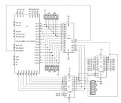
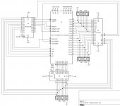
Where are you getting your information from?
There is a copy of the "Guide to Macintosh Family Hardware" scanned on Archive.org. The section about the Portable's memory configuration starts on page 205. Here is a relevant quote from page 206:
The internal memory expansion card plugs into a 50-pin connector that provides for 23
address lines, 16 data lines, plus control signals and power. When the MC68HC000 writes
data to the internal memory expansion card, it puts an address in the range $10 0000 to
$8F FFFF on the address bus. The CPU GLU custom IC decodes this address as a request to
address expansion RAM. Logic on the RAM expansion card further decodes the address
and enables the appropriate RAM ICs. Because the Macintosh Portable hardware can
address a maximum of 8 MB of expansion RAM, the 23 address lines are all that is needed
to address all the RAM on the RAM expansion card.
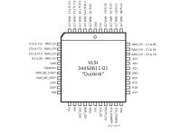
On page 208 there's the diagram of the card's pinout. The description of pin 32 is:
/DELAY.CS Chip-select signal from CPU GLU
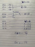
So if this description is to be believed there is a single line already provided by the onboard GLU that can be interpreted as "If this is low then the machine wants to access expansion RAM". This is where my assumption comes from that if you only have one MB of RAM on your expansion card you are completely free to ignore the state of A21-A23 beyond making sure they're all zero, and that you *also* don't care about A20; Yes, without A20 you can't tell if the machine is accessing the built-in RAM starting at 000000 verses the first 1MB of expansion RAM space at 100000... except you can, because the GLU isn't going to turn on /DELAY.CS unless A20 is on.
There's no DTACK coming to the card so the timing must be being controlled by the GLUE chip. I wonder how the RAM card is supposed to signal when the data is valid on the data bus. Or is the GLUE assuming that it will be ready after N-cycles?
I think that's a safe assumption. The computer uses the same kind of RAM chips onboard as it uses on the 1MB card (page 205) so there's no reason for it to think the expansion memory is going to be slower. Remember, the RAM chips themselves have no way to generate an "I'm ready" signal for DTACK to be referenced to, the memory controller makes that decision, and the RAM card doesn't have a controller on it.
To go even deeper about what you need here, because it looks to me like you're missing some really important parts from your first draft... Well... I'm not *super* familiar with the 68000's memory cycle so let's start here's the a reference that seemed useful:
https://hackaday.io/project/5-mc68000-computer/log/23-theory-of-ram-and-rom-modules
So what is the relationship between /UDS, /LDS, and /AS and R/W? Here's a timing diagram from the Motorola 68000 databook, I think between it and what's in that hackaday project I think I have a decent idea:

So far as the memory chips are concerned memory cycle is started when AS and UDS, LDS, or both are asserted. It looks like for RAM you may actually be able to ignore AS and just watch the UDS/LDS twins, but if you want to be kosher you might want to OR AS together with UDS and LDS together. To cut to the chase:
When /AS is low and either or both /LDS and /UDS are both LOW activate the chip select circuitry
I say "either or both" because the Apple design uses the same chip select for the hi/low chip in each bank, they're not separate.
The other thing we need to figure out is if we're preparing the chip to receive a write or assert a read on the data bus. The way the 68000 signals this is if R/W is high or low when the "chip select" combo described above is asserted. Most RAM chips use two separate signals , OE and WE. So essentially how *that* should be handled is you need to combine the CS you generate for your bank with either the straight-up or the inverted version of R/W for write or read respectively. (
Double check that to make sure I didn't flip it.) An interesting wrinkle you need to deal with is
looking at the pinout for the Apple ASIC it uses a common OE for both RAM banks. Apparently the 68000 doesn't care if it the unused 8 bits is asserted on the bus, it'll just read the half it wants, but it has a WE for each bank. Your logic needs to handle this.
Here is what I'd suggest as the solution for this. Get yourself a cheap programmer like a TL866IIplus, and some GALs. Then download and compile GALASM:
https://github.com/daveho/GALasm
I'm recommending this because it's what I'm learning to use and the default other solution, WinCUPL, is a huge pain in the rear and overkill for GALs. This is a first draft, but I think your logic solution will look something like this:
Code:
GAL16V8  ; memory decoder
MACTHING   ; done

A20 A21 A22 A23 LDS UDS RW AS DELAYCS GND
SYSPOWER NC MEMCS 245DIR 245OE RAMOE RAMWEHI RAMWELO NC VCC

245DIR = RW

/245OE = /RAMOE +
         /RAMWEHI +
         /RAMWELO

/MEMCS = /DELAYCS * A20 * /A21 * /A22 * /A23 * /AS

/RAMOE = /MEMCS * RW

/RAMWEHI = /MEMCS * /RW * /UDS

/RAMWELO = /MEMCS * /RW * /LDS

DESCRIPTION

; Decoding logic to repair a 1MB Portable memory card
; I'm not sure if 245DIR should be inverted or not, need to look at direction register on card
; SYSPOWER isn't used. In theory GAL could be used in tri-state mode and SYSPOWER used for output enable?
; Don't see a lot of point in that
; Actual chip addresses need to be decoded by an external multiplexer.
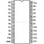
You will of course need your 74LS154 on A16-A19 to provide the individual chip selects. If the manual is correct I think you'd be safe using the /DELAY.CS output from the bus to control E0 directly, but MEMCS on the GAL will give you a fully decoded version. (Only active low when DELAY.CS is low and the address bus is between 100000 and 1FFFFF. If we really don't trust DELAY.CS then revise the equation for MEMCS so it activates if either/both of UDS/LDS is low. DELAY.CS almost certainly already incorporates this logic.)
Anyway, I *think* that'd do the needful in two chips? (Note: you'd just need the GAL if you made a new card with a pair of A6C4008s.)
