• Hello MLAers! We've re-enabled auto-approval for accounts. If you are still waiting on account approval, please check this thread for more information.

Macintosh Portable SRAM card: Schematics available?

OK, here's the final pin-out of the VLSI chip.

The two 74AC245 buffers gate the data between the memory and the system memory data bus. The two 74AC240 chips invert the addresses A1-A15 and pass them to A0-A14 on the chips. SYS_POWER* is also inverted and passed back to the VLSI chip.

The VLSI chip controls the CS* line on pairs of chips the upper and lower bytes being selected by two other lines.

The RAM OE* line is common for all chips.
 

Dunkirk-small.jpg

 
Last edited by a moderator:
ok that looks about how I expected it to. Each pair is likely to be the Upper and Lower. Now im still trying to decipher which read line is being selected, Upper or lower. 

 
Last edited by a moderator:
ok that looks about how I expected it to. Each pair is likely to be the Upper and Lower. Now im still trying to decipher which read line is being selected, Upper or lower. 
Basically, there's nothing there which can select it. The 245s are straight through connections as are most of the address lines (via inverters).

Given that I think only the address decode part of the chip is fried I'm looking at only replacing that for the time being, using a 74HC154.

This is what I'm thinking about...

If A21, A22 or A23 are high they inhibit the control of _Y0-_Y14 by _E0, which is an inverted A20. So, if A21, A22 and A23 are low and A20 is high then A16-A19 are demultiplexed and control the _CS pairs, pulling them low.

IMG_1859.jpg

IC-CD74HC154EN-2-800x800.jpg

It may need a pull-down resistor on _E1 though.

 
Last edited by a moderator:
So, devil's advocate here: instead of trying to make a replacement for the dead ASIC for this card (if all you want is 1MB) would it make more sense to just cook up a new card using a pair of AS6C4008s and send it off to a PCB puppy mill? You only need to generate two chip selects instead of a million for the same amount of RAM. If you have access to a PLD programmer that can handle obsolete GALs like the 16v8 it'd be easy to fit all the necessary logic into one.

(If you want to live dangerously you could probably do without the '245 buffers on such a card; since you're not fanning the databus out to 16 separate device my gut feeling is it'd be fine.)


The 245s are controlling the direction of the data flow to/from the data bus. I imagine making sure that the chip select is highly controlled might work, but for SRAMs that also signals the low-power mode for the chip.

 
The 245s are controlling the direction of the data flow to/from the data bus. I imagine making sure that the chip select is highly controlled might work, but for SRAMs that also signals the low-power mode for the chip.
No. The direction line on a '245 is to tell *it* whether it's passing data from "left to right" or "right to left"; the other control line on it, OE, tells it to actually pass the pin state in the chosen direction or to tri-state and stay quiet. It doesn't *control* anything. In short, its DIR signal is going to be synced up with whether the CPU is requesting a read or write, and OE is going to be synced up with chip select for the RAM chip(s) in the bank. *IF* you have a device that might create noise on the bus when it's not selected then having the buffer there is pretty important, but I don't think that's going to be an issue with RAM chips. I'd say with 90-something percent confidence it's just there for fan-out/signal integrity.

Note: Not that I don't favor having buffers "just 'cause", I included a '245 on the databus of the RAM/ROM card I made for my old Tandy, and it only has 2 devices behind it (well, three if you count the "parasite" calendar chip), but technically speaking if you had a 1MB card consisting of two 512k chips, one each on the even and odd halves of the data bus, then that *one* chip actually imparts exactly the same load on the bus as the '245 does. If instead you decided to go for the gold and build an 8MB card using 8 AS6C8008s, four each on each bus subset, then maybe the '245s would be more justifiable.

 
Last edited by a moderator:
Basically, there's nothing there which can select it. The 245s are straight through connections as are most of the address lines (via inverters).

Given that I think only the address decode part of the chip is fried I'm looking at only replacing that for the time being, using a 74HC154.

This is what I'm thinking about...

If A21, A22 or A23 are high they inhibit the control of _Y0-_Y14 by _E0, which is an inverted A20. So, if A21, A22 and A23 are low and A20 is high then A16-A19 are demultiplexed and control the _CS pairs, pulling them low.

View attachment 33154

View attachment 33155

It may need a pull-down resistor on _E1 though.


Sounds like you got this all handled, Don't need me for anything. 

Let me know how you make out, hopefully it works! 

 
One comment per the proposed solution for providing the "decoding" of A21-23; the diode thing might work, but a 3-input NOR gate like a 74HC4075 would probably be more kosher. (Or you could use a triple-input NOR gate; attach its input to the "high" enable line on the '154 instead of "low enable") I'm not even sure you need to decode A20, because according to the manual that signal "DELAY_CS" is meant as an enable for the whole card; if it's telling the truth then that will go low only when the machine is above the built-in 1MB of RAM, so I'd think you could just use that signal directly for the "low enable".

(* This is of course assuming the manual actually does tell the truth.)

Convenient part about using a NOR part instead of an OR is you can use its extras as inverters.

 
Last edited by a moderator:
Apple specs invariably call for buffering lines for PDS cards (and by extension, the memory bus in the Luggable) as close to the connector as is practical.

DCaDftMF3e pp. 444-453 covers RAM expansion cards for both Luggables.

p.447 "buffering of the address bus and data bus is important to reduce capacitive loading."

p.449 Table 20-1 lists A1-A23 and D0-D15 as unbuffered.

So, go figure? ::)

p.275 has a tidbit in the RAM section of Chapter 12 Overview of Macintosh PDS Computers:

"The Macintosh Portable has separate RAM buffers for sound and video and does not have a disk-speed controller; therefore, it does not share its system RAM with other devices." That's in comparison to description just above of RAM in the SE.

Happy to see so much activity here. [:)]

 
Actually, I think I can use a 74xx240 to do all the upper address line decoding.

Connect _E0 to ground, connect A21, A22 and A23 to I0, I1 and I2. Connect _O0, _O1 and _O2 to I3 and the _O3 output to _E1. Then connect A20 to I4. The _O4 signal can then be used to directly control _E1 on the 74HC154. The only worry is the timing. Would going through all those gates take too long?

The advantage here is that I can then use the inverted SYS_POWER line to drive the _E2 input to the 74HC154 to select the low-power mode when the machine is sleeping or shut down, and it's a two chip solution.

 
Last edited by a moderator:
Here's the first draft of the address decode circuit. Looking into the problem, it might be best to replace all the other functionality as well. I'd replace the chip with a PLCC-44 socket and fit a daughter board using a Wilmslow 9303 adapter.

Circuit-Diagram-v1.jpg

 
One comment per the proposed solution for providing the "decoding" of A21-23; the diode thing might work, but a 3-input NOR gate like a 74HC4075 would probably be more kosher. (Or you could use a triple-input NOR gate; attach its input to the "high" enable line on the '154 instead of "low enable") I'm not even sure you need to decode A20, because according to the manual that signal "DELAY_CS" is meant as an enable for the whole card; if it's telling the truth then that will go low only when the machine is above the built-in 1MB of RAM, so I'd think you could just use that signal directly for the "low enable".

(* This is of course assuming the manual actually does tell the truth.)

Convenient part about using a NOR part instead of an OR is you can use its extras as inverters.


There's no DTACK coming to the card so the timing must be being controlled by the GLUE chip. I wonder how the RAM card is supposed to signal when the data is valid on the data bus. Or is the GLUE assuming that it will be ready after N-cycles?

Given that SRAM chips take longer for the data to be ready after the /CS line is enabled than the /OE I wonder if the /CS_DELAY line is asserted first, and then sometime later /AS which should cause the /OE lines to go low. But that would make no sense as the address lines aren't valid until /AS goes low, so there's no way of knowing which /CS lines to pull down.

The alternative is that the /CS_DELAY line is there to activate the /OE on the 74AC245 to allow data in or out of the card.

Where are you getting your information from?

 
Where are you getting your information from?
There is a copy of the "Guide to Macintosh Family Hardware" scanned on Archive.org. The section about the Portable's memory configuration starts on page 205. Here is a relevant quote from page 206:

The internal memory expansion card plugs into a 50-pin connector that provides for 23
address lines, 16 data lines, plus control signals and power. When the MC68HC000 writes
data to the internal memory expansion card, it puts an address in the range $10 0000 to
$8F FFFF on the address bus. The CPU GLU custom IC decodes this address as a request to
address expansion RAM. Logic on the RAM expansion card further decodes the address
and enables the appropriate RAM ICs. Because the Macintosh Portable hardware can
address a maximum of 8 MB of expansion RAM, the 23 address lines are all that is needed
to address all the RAM on the RAM expansion card.

On page 208 there's the diagram of the card's pinout. The description of pin 32 is:

/DELAY.CS Chip-select signal from CPU GLU

So if this description is to be believed there is a single line already provided by the onboard GLU that can be interpreted as "If this is low then the machine wants to access expansion RAM". This is where my assumption comes from that if you only have one MB of RAM on your expansion card you are completely free to ignore the state of A21-A23 beyond making sure they're all zero, and that you *also* don't care about A20; Yes, without A20 you can't tell if the machine is accessing the built-in RAM starting at 000000 verses the first 1MB of expansion RAM space at 100000... except you can, because the GLU isn't going to turn on /DELAY.CS unless A20 is on.

There's no DTACK coming to the card so the timing must be being controlled by the GLUE chip. I wonder how the RAM card is supposed to signal when the data is valid on the data bus. Or is the GLUE assuming that it will be ready after N-cycles?
I think that's a safe assumption. The computer uses the same kind of RAM chips onboard as it uses on the 1MB card (page 205) so there's no reason for it to think the expansion memory is going to be slower. Remember, the RAM chips themselves have no way to generate an "I'm ready" signal for DTACK to be referenced to, the memory controller makes that decision, and the RAM card doesn't have a controller on it.

To go even deeper about what you need here, because it looks to me like you're missing some really important parts from your first draft... Well...  I'm not *super* familiar with the 68000's memory cycle so let's start here's the a reference that seemed useful:

https://hackaday.io/project/5-mc68000-computer/log/23-theory-of-ram-and-rom-modules

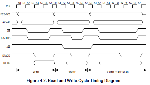
So what is the relationship between /UDS, /LDS, and /AS and R/W? Here's a timing diagram from the Motorola 68000 databook, I think between it and what's in that hackaday project I think I have a decent idea:


So far as the memory chips are concerned memory cycle is started when AS and UDS, LDS, or both are asserted. It looks like for RAM you may actually be able to ignore AS and just watch the UDS/LDS twins, but if you want to be kosher you might want to OR AS together with UDS and LDS together. To cut to the chase:

When /AS is low  and either or both /LDS and /UDS are both LOW activate the chip select circuitry

I say "either or both" because the Apple design uses the same chip select for the hi/low chip in each bank, they're not separate.

The other thing we need to figure out is if we're preparing the chip to receive a write or assert a read on the data bus. The way the 68000 signals this is if R/W is high or low when the "chip select" combo described above is asserted. Most RAM chips use two separate signals , OE and WE. So essentially how *that* should be handled is you need to combine the CS you generate for your bank with either the straight-up or the inverted version of R/W for write or read respectively. (Double check that to make sure I didn't flip it.) An interesting wrinkle you need to deal with is looking at the pinout for the Apple ASIC it uses a common OE for both RAM banks. Apparently the 68000 doesn't care if it the unused 8 bits is asserted on the bus, it'll just read the half it wants, but it has a WE for each bank. Your logic needs to handle this.

Here is what I'd suggest as the solution for this. Get yourself a cheap programmer like a TL866IIplus, and some GALs. Then download and compile GALASM:

https://github.com/daveho/GALasm

I'm recommending this because it's what I'm learning to use and the default other solution, WinCUPL, is a huge pain in the rear and overkill for GALs. This is a first draft, but I think your logic solution will look something like this:
 

Code:
GAL16V8  ; memory decoder
MACTHING   ; done

A20 A21 A22 A23 LDS UDS RW AS DELAYCS GND
SYSPOWER NC MEMCS 245DIR 245OE RAMOE RAMWEHI RAMWELO NC VCC

245DIR = RW

/245OE = /RAMOE +
         /RAMWEHI +
         /RAMWELO

/MEMCS = /DELAYCS * A20 * /A21 * /A22 * /A23 * /AS

/RAMOE = /MEMCS * RW

/RAMWEHI = /MEMCS * /RW * /UDS

/RAMWELO = /MEMCS * /RW * /LDS

DESCRIPTION

; Decoding logic to repair a 1MB Portable memory card
; I'm not sure if 245DIR should be inverted or not, need to look at direction register on card
; SYSPOWER isn't used. In theory GAL could be used in tri-state mode and SYSPOWER used for output enable?
; Don't see a lot of point in that
; Actual chip addresses need to be decoded by an external multiplexer.
You will of course need your 74LS154 on A16-A19 to provide the individual chip selects. If the manual is correct I think you'd be safe using the /DELAY.CS output from the bus to control E0 directly, but MEMCS on the GAL will give you a fully decoded version. (Only active low when DELAY.CS is low and the address bus is between 100000 and 1FFFFF. If we really don't trust DELAY.CS then revise the equation for MEMCS so it activates if either/both of UDS/LDS is low. DELAY.CS almost certainly already incorporates this logic.)

Anyway, I *think* that'd do the needful in two chips? (Note: you'd just need the GAL if you made a new card with a pair of A6C4008s.)

 
Last edited by a moderator:
(Note of course all of the above comes with the usual disclaimers, IE, I probably have no idea what I'm talking about, don't do it, you'll melt your computer, etc.)

 
Actually a GAL is a good idea. It's need a 20V10 for the number of inputs.
 

It'll still need the 244 and the pull-ups but should put everything else into the GAL, making a three chip solution to the problem.

 
Actually a GAL is a good idea. It's need a 20V10 for the number of inputs.
Why do you think you need a 20v10, IE, which inputs did I miss? Remember, A16-A19 don't need to go to the GAL because it's not demultiplexing addresses within the 1MB window, it only needs to produce a chip select to signal the demultiplexer to output its selection and the shared read/write signals, and the relevant input pins for that are:

A20-23 (4)

DELAY.CS

/LDS

/UDS

/AS

R/W

That's nine, and if we chuck in SYSPOWER which we probably won't use that's 10. A 16v has 8 "input only" pins, but if you're not using the GAL's clock or tristate functions (I don't see a need for them) you can use pins 1 and 11 as inputs, so it seems to me we're covered.

In principle at least if you wanted to use a pair of 22v10s we're *this* close to not needing the 74154; you need that mind-boggling 16 chip select outputs, since the 22v10 has 10 output registers you could split that 8/8 between a pair; the problem is we also need this:

245_DIR

245_OE

RAM_OE

RAM_WE_HI

RAM_WE_LO

That's one too many. The only way I see around that would be to spin off "245_DIR". How are the 245s on the databus wired? (IE, which side is facing the chips and which the bus connector.) I assume 245_DIR just directly shadows R/W and is just run through the ASIC to buffer it, but I suppose it could be inverted. (Although a chart in the Backlit Portable dev guide implies it's not.)

and the pull-ups
There are CMOS versions of the 74HC154, so I'd probably say do that and ditch the pull-ups. Granted they're not super easy to find, the '154 is kind of an obsolete part. If you genuinely can't find one maybe a pair of 74HC138s would be preferable. (Connect them to A16-A18 and have the GAL generate a separate CS for each of them, or play games with the E inputs to use A19 to directly cascade them, per the manual.)

FWIW, I tracked down the dev notes for both the backlit and non-backlit portables, and unfortunately they're kind of a mess. The one for the non-backlit portable looks like it suffered some sort of trans-genetic mutation in the typesetting process so the pinout description for the memory port is obviously wrong. (It labels the /UDS pin as a clock output, for instance.) Unfortunately the critical thing that suffered is it completely garbled the description of /DELAY.CS. Adding to the confusion, the Backlit Portable says that /DELAY.CS was replaced with a /REFRESH pin without really explaining what it was used for previously so...

TL;DR, I'm sold on thinking it might not be worth paying attention to /DELAY.CS and instead the generation of /MEMCS on the GAL should rely solely on the /AS + /LDS and/or /UDS transitions and full decoding of /A20-/A23.

@techknight: When you designed that RAM card you did it for the backlight portable, correct? Did you generate your RAM chip selects just using /AS + /LDS + /UDS + Address Lines or did you rely on the muddledly-documented /RAM.CS and /REFRESH lines at all?

 
Last edited by a moderator:
My card was designed to work in both machines, and no, I never messed with Apples muddied garbage select and control lines. 

I simply designed the card to work on the 68K bus as a generic 68K bus, and handled all the decoding/logic in the card itself. 

It seemed to work fine, I never had any errors. I didnt even listen to the power signal either I dont believe. 

Also all lines from A16-A19 need to be decoded as well, because we are not working on the megabyte barriers, we are working on 32Kx16 barriers (each chip being 32K, and at 2 chips total 16 bits, so 64KBytes)

Address strobe gets asserted when a valid address is on the bus. Thats when the decoder circuit activates. the Lower/Upper data strobes activate when there is valid data on the bus. So thats when the read/write and direction control needs to activate. 

DTACK isnt that important, with fast enough RAM you can ground DTACK. (Dont do this on this card, its too old). There was an exception here, with the portable backlit model, DTACK isnt decoded past 5MB so I had to branch off an additional DTACK line from the card on a header I made, and back to a pin on the ROM slot. a PDS RAM card would not have this limitation, of course. 

 
Last edited by a moderator:
Also all lines from A16-A19 need to be decoded as well, because we are not working on the megabyte barriers, we are working on 32Kx16 barriers (each chip being 32K, and at 2 chips total 16 bits, so 64KBytes)
That's what the 74154 or a pair of 74138s is for, decoding within the 1MB window that's defined by the GAL (in the single GAL version; the GAL provides one chip select that's cascaded to the demultiplexers). The 2-GAL idea would need the GALs both listening to A16-A19; a 22v should provide just enough pins.

DTACK isnt that important, with fast enough RAM you can ground DTACK. (Dont do this on this card, its too old).
The memory card bus doesn't have DTACK on it, so my assumption is that it just goes with the onboard GLU's timing assumption and doesn't expect any kind of "I'm READY!" from the card. Your observations seem to bear this out; I do wish /DELAY.CS was better explained, however.

Here's my revised GAL code with references to DELAY.CS removed. The inside-the-window multiplexers will select when AS is low and address is between 100000-1FFFFF, and the read/write lines will activate when /UDS and /LDS go low when the memory is selected. 


Code:
GAL16V8  ; memory decoder
MACTHING   ; done

A20 A21 A22 A23 LDS UDS RW AS DELAYCS GND
NC NC MEMCS 245DIR 245OE RAMOE RAMWEHI RAMWELO NC VCC

245DIR = RW

/245OE = /RAMOE +
         /RAMWEHI +
         /RAMWELO

/MEMCS = A20 * /A21 * /A22 * /A23 * /AS

/RAMOE = /MEMCS * /UDS * RW +
         /MEMCS * /LDS * RW

/RAMWEHI = /MEMCS * /RW * /UDS

/RAMWELO = /MEMCS * /RW * /LDS

DESCRIPTION

; Decoding logic to repair a 1MB Portable memory card
; 245DIR is just a buffered version of R/W direction register on card
; A chart in the Portable (BL) dev note implies this is right
; SYSPOWER isn't used.
; Actual chip addresses need to be decoded by an external multiplexer.
; Use MEMCS as select for this multiplexer
I still think it might be preferable to just skip fixing this card and make a whole new card using a pair of 512kx8 SRAMs. It'll be a lot cleaner than going through a pile of socket adapters and you don't need the multiplexer anymore. BOM would be the GAL, three 74HC244s, two 74HC245s, two A6C4008s, and some bypass caps. 

 
Last edited by a moderator:
I realised I'd miscounted the number of inputs (should be 8 ) after I modified the schematic, so yes a 16V8 will work fine.

As for the 74HC154 they seem to be plentiful from both RS Components and Farnell, but only as SOIC packages.

As for SYS_POWER*, from what I can make out from the schematics it looks like it's there to disable hardware until the system is fully powered (i.e. not in sleep or "shut down"). Admittedly, for the RAM card is should be superfluous, though apparently the SRAM chips run in low-power mode if /CS is forced HIGH.

Anyway, here's the latest schematic (with the bigger GAL, which I can swap out). I need to create a footprint for the PLCC adapter rather than using the placeholder SMT one I have at the moment.

Dunkirk-Replacement.jpg

 
The BOM for this design would be a Winslow 9303 adapter, 74xx244, 74HC154, 16V8, a PLCC-44 socket a DIP socket and three resistor networks.

 
Back
Top