
I’m so glad it worked!Golden Potato, I've tried your proposed ROM patch and can confirm that it works as intended! Now my Mac 512K boots with a 1.5MB RAM expansion and the ROM-INATOR. Once again, you nailed it!
-
 Hello Guest! We're hosting a challenge to welcome vintage Intel macs to the MLA during the month of July! See this thread for more information.
 -
We've made some quality of life improvements to the Trading Post. More info here.
You are using an out of date browser. It may not display this or other websites correctly.
You should upgrade or use an alternative browser.
You should upgrade or use an alternative browser.
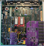
Early Macintosh home brew 4MB memory upgrade board development
- Thread starter Golden Potato
- Start date
A little update: The 74259 sub-circuit can now be activated without causing issues. The Mac boots normally, recognizes the RAM expansion, and seems to function correctly. The only changes I made since the prototype build were to add pull-ups to A22 and A23 and patch the code of the ROM-INATOR ROM at 0x0003F0. Since this circuit was intended for the Mac 512KE (MacPlus ROM) ,I'll keep it activated and set as the default.It looks like it brings pin 15 high/disabled for writes to 0x200000-0x300000. I don't know why off the top of my head though.

Last edited:
The macSnap board doesn't use pull-ups for A21, A22, A23. So, I guess I use it at some point testing the circuit. I eliminate them and everything works fine.A little update: The 74259 sub-circuit can now be activated without causing issues. The Mac boots normally, recognizes the RAM expansion, and seems to function correctly. The only changes I made since the prototype build were to add pull-ups to A22 and A23 and patch the code of the ROM-INATOR ROM at 0x0003F0. Since this circuit was intended for the Mac 512KE (MacPlus ROM) ,I'll keep it activated and set as the default.
View attachment 78727
Yes, eventually.Yes yes I want =)
Would there be ready to use builds for sale eventually?
Already took 512k logic board on my desk
A little update: The 74259 sub-circuit can now be activated without causing issues. The Mac boots normally, recognizes the RAM expansion, and seems to function correctly. The only changes I made since the prototype build were to add pull-ups to A22 and A23 and patch the code of the ROM-INATOR ROM at 0x0003F0. Since this circuit was intended for the Mac 512KE (MacPlus ROM) ,I'll keep it activated and set as the default.
View attachment 78727
I'm trying once again to understand this portion of the circuit for the MacSnap.
The output of the 74LS259 controls OEb of the 74LS253.
OEb of the 74LS253 being HIGH forces its output Zb LOW.
Output Zb of the 74LS253 being LOW forces the 74LS139s to only provide CAS to either CAS2F&CAS3F (system 512K) or CAS4F&CAS5F, so only 1MB of memory is possible. CAS0F&CAS1F and CAS6F&CAS7F are disabled, so 1.5MB or 2MB are not possible.
All of this going the other way allows all CAS#F signals to be enabled, so 1.5MB or 2MB is possible.
The output of the 74LS259 is a latched bit, so it maintains its output until it is changed.
Its output is changed only when the system writes to an address within the range 0x200000-0x27FFFF or 0x280000-0x2FFFFF (A19 being the deciding factor between the two ranges).
Writing to 0x200000-0x27FFFF sets the output of the 74LS259 to LOW which enables CAS provisions for all CAS#F lines.
Writing to 0x280000-0x2FFFFF sets the output of the 74LS259 to HIGH which disables CAS0F&CAS1F and CAS6F&CAS7F.
Reading from these address ranges makes no changes to this latch.
Was there any special software which came with the MacSnap board? Perhaps the purpose of this memory mapped latch is for a software controlled configuration change?
On another train of thought following Builder68's theory: Maybe the Plus ROM does something funny in these address ranges? In a Ghidra disassembly of the Mac Plus ROM, is there a simple way to search for writes to specific ranges in memory (such as these two range in question)?
It's strange that the system would write to these ranges which are mirrors of RAM, so I don't think it would typically do so. In fact, a 4MB mod would not be possible, since 0x200000-0x2FFFFF lands within the 4MB memory range (0x000000-0x3FFFFF) and writes to 0x280000-0x2FFFFF will disable a portion of RAM.
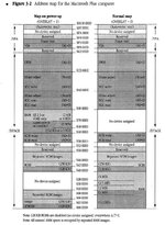
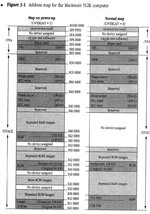
Here is the possible memory mapping and mirroring for RAM with regard to 1MB blocks:
0x000000-0x0FFFFF : 1st 1MB
0x100000-0x1FFFFF : 2nd 1MB or 1st mirror of 0x000000-0x0FFFFF
0x200000-0x2FFFFF : 3rd 1MB or 2nd mirror of 0x000000-0x0FFFFF or 1st half of mirror of 0x000000-0x1FFFFF
0x300000-0x3FFFFF : 4th 1MB or 3rd mirror of 0x000000-0x0FFFFF or 2nd half of mirror of 0x000000-0x1FFFFF
Do you have this software? Maybe this part of the circuit has something to do with the RAM disk?There was dove Macsnap software, but that was solely for creating a RAM-disk
Dove only implemented the 74259 in 'E' board models (524E, 548E), which were advertised for the Macintosh 512KE.Was there any special software which came with the MacSnap board? Perhaps the purpose of this memory mapped latch is for a software controlled configuration change?
No software for configuration came with those boards. As JoopMac pointed out, the only software that came with all MacSnap models was an app to create RAM disks.
Quite a mystery, those memory ranges. I will try to dig into the Mac Plus disassembly looking for them. **It's strange that the system would write to these ranges which are mirrors of RAM, so I don't think it would typically do so. In fact, a 4MB mod would not be possible, since 0x200000-0x2FFFFF lands within the 4MB memory range (0x000000-0x3FFFFF) and writes to 0x280000-0x2FFFFF will disable a portion of RAM.
I haven't yet populated the RAM ICs to reach 3.5MB of RAM expansion; that's probably why it's working with 1.5 MB and the 74259 enabled.
I read something here about memory map differences between the Mac Plus and the Mac 512K, and something about the RAM space not being contiguous in 512KE models with certain RAM expansions.
Maybe the RAMDisk app makes use of those noncontiguous RAM spaces... I think we need to start digging in detail into the memory map of the 512KE when a RAM expansion is implemented.
Attachments
Last edited:
Its this:
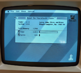
Thank you, it works as expected with 2MB of RAM. What the app does is setting a RAM disk of the preferred size and copying a selected folder into it during boot-up. It also lets you reserve a desired RAM size for cache.
Here is the same link on Internet Archive from before MacGUI locked down their articles to signed in users only: https://web.archive.org/web/20220711020335/https://macgui.com/news/article.php?t=470I read something here about memory map differences between the Mac Plus and the Mac 512K, and something about the RAM space not being contiguous in 512KE models with certain RAM expansions.
Maybe the RAMDisk app makes use of those noncontiguous RAM spaces... I think we need to start digging in detail into the memory map of the 512KE when a RAM expansion is implemented.
The noncontiguous-ness isn’t a problem for 512Ke systems, but it is for non-e systems. It’s not a hardware memory map difference, since both types of 512K systems are identical. The issue is with the ROM.
The original 64K ROM has a pointer to the screen buffer in RAM which was coded to be found in only two places which was the top of RAM in 128K or 512K systems. If RAM was added above 512K and the hardware adjusted to put the screen buffer at the new top of RAM (should happen automatically due to address line pull up resistors), the software in the ROM still points to the old location, so the screen buffer was essentially fixed at that point in memory due to the software running in the ROM. The article mentions at least one memory upgrade company building a ROM patch straight onto the upgrade board.
But all of those problems went away with the release of the 128K ROM (Mac Plus ROM). Now the ROM detects all memory and points the screen buffer to the top of the memory found.
At least that’s how I interpreted the article!
Your interpretation is correct! So in summary, the non-contiguous memory problem in early Macs was primarily due to a limitation in the original ROM design. The introduction of the 128K ROM, with its ability to dynamically adjust the screen buffer pointer, addressed this issue. Therefore, it seems the 74259 subcircuit is not directly involved in this particular problem.The noncontiguous-ness isn’t a problem for 512Ke systems, but it is for non-e systems. It’s not a hardware memory map difference, since both types of 512K systems are identical. The issue is with the ROM.
The original 64K ROM has a pointer to the screen buffer in RAM which was coded to be found in only two places which was the top of RAM in 128K or 512K systems. If RAM was added above 512K and the hardware adjusted to put the screen buffer at the new top of RAM (should happen automatically due to address line pull up resistors), the software in the ROM still points to the old location, so the screen buffer was essentially fixed at that point in memory due to the software running in the ROM. The article mentions at least one memory upgrade company building a ROM patch straight onto the upgrade board.
But all of those problems went away with the release of the 128K ROM (Mac Plus ROM). Now the ROM detects all memory and points the screen buffer to the top of the memory found.
At least that’s how I interpreted the article!
I finally had the time to fully assemble the second version of the prototype boards. Stock and MacPlus-style refresh cycle modes work flawlessly as before, now with full 4MB!
I promise to make the fabrication files for version 2 of these boards available on GitHub soon.
Just for fun, I'm working on a third prototype to refine several aspects, including making it fully compatible with a Macintosh 128K (equipped with MacPlus ROMs or a ROM-INATOR) by simply adjusting settings on a DIP switch. While the current prototype can function with a Mac 128K by installing some additional cables, only 3.5MB would be available.
To address this, I will include an eighth RAM IC. Additionally, with 4MB of memory on the expansion board, I believe it would be beneficial to add an option to include or exclude the system memory bank within the 4MB range through a DIP switch when the boards are installed on Mac 512K /Ke models.
I see no reason to maintain three selectable refresh modes in the future. Since the system cycle refresh works so well with the selected DRAM ICs, it will be the only option, thus reducing the need for some components and signals from the motherboard.
Next up, I'm going to investigate how easy it would be to add one cool and handy feature from the Mac's-a-Million RAM upgrade board. It allows you to boot with just the stock RAM if you hold down the mouse button while starting up.
I'm pretty sure that the retro community will soon be saved from the hassle and expense of finding a rare and costly MacRescue board on eBay to enable full 4MB of RAM paired with a SCSI interface on an Early Mac!
I hope demik finds new strengths and finally makes a breakthrough in his SCSI project for the early Macs in the near future!
Attachments

Am i right that there is a patched ROMINATOR ROM for the RAM expansion + ROM boot option?
Similar threads
- Replies
- 22
- Views
- 2K
- Replies
- 61
- Views
- 25K
- Replies
- 0
- Views
- 2K
- Replies
- 203
- Views
- 54K