• Updated 2023-07-12: Hello, Guest! Welcome back, and be sure to check out this follow-up post about our outage a week or so ago.

SuperMac Spectrum 24/V Display Problems

jmacz

Well-known member
Finally getting back to this after putting it aside to work on many things, including finally fixing my SuperMac Spectrum PDQ+:


Based on the learnings from fixing that particular video card, I quickly pointed my test program at this Spectrum 24 Series V card. I have been primarily focused on resolving the issue with the red columns during boot. But after running my test program, this card is seriously damaged and has issues across red, green, blue... in fact, running my test against a small 8 pixel by 8 pixel square region on the frame buffer, 56 of the 64 pixels had errors -- as in what I wrote was not what made it to the frame buffer. FUN!

Hopefully will get some time during the evenings this week otherwise will hopefully get some time to dig in further this weekend. This is my last problematic SuperMac video card remaining. :)
 

jmacz

Well-known member
I utilized my test programs from debugging my Spectrum PDQ+ to finally put together SuperMac's layout for their VRAM chips at 24bit on the Spectrum 24 series V (and the same layout is used for the Spectrum 24 series IV and Spectrum 24 PDQ+, also probably the same for the Thunder variants that have the same PCB layout).

Frame Buffer Addresses

Each 24bit pixel is a 32bit value of the format 0x00RRGGBB, so each pixel takes up 4 bytes of memory. But for the rest of this post, think of it this way:
  • 32bit Value In Binary: xxxx xxxx xxxx xxxx xxxx xxxx xxxx YYZZ
  • Where
    • ZZ = 2 bits for the byte of the RGBA.. 00=A, 01=R, 10=G, 11=B
    • YY = 2 bits for the column identifier.. 00=Column0, 01=Column1, 10=Column2, 11=Column3... (groups of 4 columns)
    • xxxx xxxx xxxx xxxx xxxx xxxx xxxx = the rest of the address
Examples:
  • xxxxxxxxxxxxxxxxxxxxxxxxxxxx0011 = the blue byte in a column 0
  • xxxxxxxxxxxxxxxxxxxxxxxxxxxx0101 = the red byte in a column 1
  • xxxxxxxxxxxxxxxxxxxxxxxxxxxx1010 = the green byte in a column 2
  • xxxxxxxxxxxxxxxxxxxxxxxxxxxx1111 = the blue byte in a column 3
Thus:
  • Every pixel's first byte where the pixel appears in the columnNumber % 4 == 0 has an address that ends with 0x0
  • Every pixel's first byte where the pixel appears in the columnNumber % 4 == 1 has an address that ends with 0x4
  • Every pixel's first byte where the pixel appears in the columnNumber % 4 == 2 has an address that ends with 0x8
  • Every pixel's first byte where the pixel appears in the columnNumber % 4 == 3 has an address that ends with 0xc
The Layout in 24 bits

Spectrum Memory Layout.png

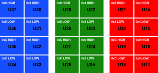
The black labels represent the VRAM labels on the PCB. The info in white represents the column/byte that that VRAM is responsible for. More examples:
  • U37 VRAM Chip
    • For addresses where the column ID mask is 0x8, this chip generates the most significant 4 bits of the blue color.
  • U25 VRAM Chip
    • For addresses where the column ID mask is 0x0, this chip generates the least significant 4 bits of the green color.
  • U19 VRAM Chip
    • For addresses where the column ID mask is 0xc, this chip generates the most significant 4 bits of the red color.
Put another way, if you're debugging and you find an unexpected pixel value (for the red channel) for the 32 bits of pixel data that starts with frame buffer address 0x???????4, then you know that particular pixel's value is held within:
  • VRAM Chip U14 for the high 4 bits of the red channel
  • VRAM Chip U15 for the low 4 bits of the red channel
This is what I used to narrow down the actual VRAM chip that was causing my PDQ+ issue. And what I'm hoping to utilize to narrow down the issues with my Spectrum 24 Series V which is what this thread is about.
 
Last edited:

jmacz

Well-known member
Quick addition for future readers (forgot to mention in my previous post).

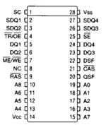
As mentioned above, a single VRAM chip (in 24bit mode) is responsible for 4 bits of a color value for a specific column. Looking at those 4 bits of data, these are the pins on the VRAM chip responsible for sending each bit to the DAC:
  • Any given VRAM chip
    • Pin 2 (SDQ1) - 0x1 - 0001
    • Pin 3 (SDQ2) - 0x2 - 0010
    • Pin 26 (SDQ3) - 0x4 - 0100
    • Pin 27 (SDQ4) - 0x8 - 1000
So based on the address, you can narrow it down to the specific pin on a specific VRAM chip.
 

MacOSMonkey

Well-known member
Very useful info! Nice charts!

Thunder, Spectrum PDQ+, Spectrum/24 IV and Spectrum/24 V are all very similar designs - mostly just marketing designations/rebranding and/or gimping (in the case of the PDQ+). Also, in terms of how things get moved around in accelerated mode -- one of the advantages of Squid was that it could move 4 pixels at a time (32-bits in 8-bit mode or 96-bits in 24-bit mode). There was also a 1x packed RGB mode, but maybe that was only on the Spectrum 8*24 boards (regular Nubus and IIsi).
 

jmacz

Well-known member
Yeah, this card's a mess.

Wrote a program to write some algorithmic values to the frame buffer and read it back in. There's bad values all over the place (across most of the chips). I can't imagine all the chips are bad so it's probably the address lines. Wrote another function to read the values one time and store them in memory, then keep reading the values over and over (100s of iterations) and I'm getting inconsistent reads even without writing again to the frame buffer.
 

MacOSMonkey

Well-known member
Right - so one way to track this one down would to write to a known address on the 68K side and wire the address bus on the card to see how the address is being decoded.

You know the RAM mapping. Try to reproduce the problem starting at the base address -- like $E0000100 -- it's going to be super-slot address + the bit-field extract protection buffer. Then, systematically toggle each address bit, write continuously, and see what address the board sees. You can use your nubus debugger and also grab it from the RAM. Look for solder fractures, device failures (like the one on the other board, etc.). If it's an address line problem, you should be able to find the problem(s) relatively quickly. Also, for the fine-pitch TQFP's, make sure none of the pins are mashed together.
 

jmacz

Well-known member
Need to order some more probe clips. I've got eight small ones but need eight more to take advantage of all 16 channels I have. Even then, going to be annoying as I can't watch more than 16 signals at a time.

The VRAM chips are 9bits (A0-A8 on the falling edge of RAS) for DRAM row followed by 9bits (A0-A8 on the falling edge of both RAS and CAS) for DRAM column. Need to figure out how that's mapped to a 32bit frame buffer address. I'll monitor my now working PDQ+ to figure out the mapping and then try on the S24V.

Will also trying watching the nubus lines at some point, on both sides of the bus transceivers, but will need to get more familiar with nubus before I can do that. Also going to be annoying as there's 32 address lines on Nubus yet my logic analyzer only has 16 channels.
 

jmacz

Well-known member
BTW, lost some time today because all of a sudden I was getting grayscale only on my S24V but I didn't notice. Spent time debugging why all of a sudden my red channel was gone, until I realized the ghosts in this card flipped the DAC into grayscale mode. Grr.. Just added tracing of those S1/SO pins on the DAC to see where that comes from as that is also clearly not working right. Either more traces that are bad or something's wrong with the Nubus lines as well (likely since the connector was damaged) and the wrong setting got applied during boot. Weird part is I tested resistance and for shorts across all the Nubus pins and saw nothing out of the norm.
 

MacOSMonkey

Well-known member
The color/gray problem might point to a number of issues:

1. Bad data in a driver call. So, the driver misinterprets a color/gray flag in the paramBlock for SetMode -- or something like that.
2. PRAM gremlin as a consequence of whatever is going on with the card.
3. Some other random issue.

I would think this kind of problem is more driver-related with bad data, since the card doesn't just flip into gray mode. It would have to be set up that way.

Maybe zap PRAM just to make sure.

In terms of the address problem -- you could use a bank of LEDs or just look at 8 bits at a time on your scope.
 

jmacz

Well-known member
In terms of the address problem -- you could use a bank of LEDs or just look at 8 bits at a time on your scope.

I'm stepping through via MacsBug but that's not going to freeze the card so the LEDs would blink too fast for me to observe the values.
 

jmacz

Well-known member
No debugging progress to report as I've been busy with work but I was able to utilize my logic analyzer to figure out how the 9 address bits map to the frame buffer.

Referring back to this diagram:

Spectrum Memory Layout.png

Each of those boxes is a MT42C4256 VRAM chip (24 in total). The pin assignment of each VRAM chip:

Screenshot 2024-07-12 at 5.40.31 PM.png
The 9 address lines are A8 through A0. These address lines are used for both a row address and a column address (this is not screen rows/columns but for addressing the VRAM memory). With 9 bits, that's 512 values. 512 rows and 512 columns = 262,144 possible addresses and for EACH address, the chip stores 4 values which are handled via pins DQ1 through DQ4.

The RAS pin (row address strobe) and the CAS pin (column address strobe) are utilized during read/write cycles to denote when these address pins are being used to identify a row vs a column.

There are three different RAS signals coming from the SMT02S chip, one for each of BLUE, GREEN, RED. So all the RAS pins on the BLUE chips are connected, all the RAS pins on the GREEN chips are connected, and all the RAS pins on the RED chips are connected. This allows the SMT02S to choose which bank of VRAM chips it is talking to (the BLUE ones, the GREEN ones, or the RED ones).

There are four different CAS signals coming from the SMT02S chip, one for the 0x0, 0x4, 0x8, 0xC columns. So all the 0x0 chips have their CAS connected to each other, same goes for the 0x4, 0x8, 0xC chips. This allows the SMT02S to further choose which 2 of the 8 VRAM chips in each bank it is addressing.

As an example, the SMT02S could pull down the RED RAS line, and then pull down the 0x8 CAS line to specifically target chips U21 and U20 for a cycle/operation. The SMT02S does NOT need to further differentiate between U21 and U20 because those two chips represent the high 4 bits and the low 4bits of a byte, and the cycle/operation is operating on bytes (8 binary values at a time, 4 from each chip).

Mapping a frame buffer address to screen coordinates or a VRAM 9-bit address

I have only been playing with the mapping in 24 bit color at a resolution of 1024x768. The following is valid only in this mode.

Frame buffer base address for this video card (sitting in nubus slot E): 0xe0100000
Row bytes for this video card: 4096

Example frame buffer address: 0xe0107ff5
Offset after removing the base: 0x00007ff5
Offset divide by 4 to account for 4 bytes per pixel: 0x000007ff5 >> 2 = 0x00001ffd
Row pixels divide by 4 to account for 4 bytes per pixel: 4096 or 0x0001000 >> 2 = 0x00000400

Screen X Coordinate: 0x00001ffd % 0x00000400 = 1021
Screen Y Coordinate: 0x00001ffd / 0x00000400 = 7

In 24bit 1024x768 resolution, VRAM rows begin at x00000080.

VRAM Memory Column: (0x00001ffd % 0x00000800) >> 2 = 0x000001ff (A8 through A0 as 111111111)
VRAM Memory Row: (0x00001ffd / 0x00000800) + 0x00000080 = 0x00000083 (A8 through A0 as 100000011)
VRAM Chip Bank: 0x000007ff5 & 0x00000003 = 0x00000001 = RED Bank
VRAM Chip Column: 0x000007ff5 & 0x0000000c = 0x00000004 = 0x4 column chips = U14 and U15

The VRAM Memory Column has a shift by 2 because of the 0x0/0x4/0x8/0xC column specific chips. The VRAM Chip Bank calculation is basically acknowledging that each pixel is represented by 4 bytes and the first byte is alpha (?), second byte is red, third byte is green, and fourth byte is blue.

Just leaving this here for anyone debugging their Spectrum 24 IV/V/PDQ+/Thunder in the future.
 

MacOSMonkey

Well-known member
Great job! Very thorough!

Here is some additional information to add to your post:
Micron Datasheet (at Jameco) for MT42C4256 : https://www.jameco.com/Jameco/Products/ProdDS/2280415.pdf

For those who want to debug these VRAM devices, there are 28-pin SOIC chip clips that make wiring these parts to an analyzer very easy. Just clip and go - no analyzer rewiring required. There may be cheaper ones, but here is an example: https://us.warwickts.com/68/Pomona-5437-28-Pin-SOIC-Test-Clip
It looks like the (current) price range is $20-$50+. Check ebay.

re: Alpha Channel: I don't recall any hardware alpha channel support on Thunder class boards. The upper byte isn't used. Offscreen GWorld -- yes - on Thunder/24 - up to 8Mb, but not a dedicated Alpha Channel. But, in either case, you would still need PhotoShop and it added that functionality in software, where the add-on DSP accelerator module (if your board has the extra connectors -- not on Spec/24 PDQ+, for example) would speed up certain operations. There was also a stand-alone board that did the same thing for cards that didn't support add-on modules.
 

jmacz

Well-known member
For those who want to debug these VRAM devices, there are 28-pin SOIC chip clips that make wiring these parts to an analyzer very easy. Just clip and go - no analyzer rewiring required. There may be cheaper ones, but here is an example: https://us.warwickts.com/68/Pomona-5437-28-Pin-SOIC-Test-Clip
It looks like the (current) price range is $20-$50+. Check ebay.

Yeah, was eyeballing clips but the price was so high and wasn't sure I would ever need them again.. but based on how much clipping I've been doing, might be worth the investment.
 

jmacz

Well-known member
Some progress.

After figuring out the address mapping (previous post) and getting more familiar with the read/write cycles of the VRAM chip during that address mapping exercise via the spec sheet, and observing the behavior on a working card (PDQ+), I took those learnings and put my faulty S24/V on the logic analyzer to check the behavior of the VRAM address lines.

What I was noticing from my test programs was that U14, U15, U22, U23, U30, U31 seemed to not be generating errors.

Now looking more closely via my logic analyzer on U14 and U15, everything seems to be ok. The address lines have the proper values during my tests and same with the RAS/CAS signals going to those chips.

But then I took a look at U21 and saw a clear problem. Although the RAS signal and the VRAM address lines seem to be right when a value is being written to VRAM, the CAS signal is missing. The signal isn't dead, there's activity, but it's wrong! I then took a look at U19 and U16 as well, bad CAS signals also.

I had mentioned in an earlier post that there are four CAS lines, which I'm calling 0x0 CAS, 0x4 CAS, 0x8 CAS, and 0xC CAS. One of them is functioning properly (0x4) but the other three (0x0, 0x8, 0xC) are not. They have signals but they are wrong. This explains why the six chips I mentioned earlier (U14, U15, U22, U23, U30, U31) seem to be working correctly as they utilize the 0x4 CAS line. The rest of the chips use the 0x0, 0x8, 0xC CAS lines and thus are having issues. The signal on those faulty CAS lines again do have some activity so if a write operation lands at the right time, it works, but because they are wrong, it also doesn't work most of the time.

These CAS signals are connected to:

SMT-02S
  • Pin 125 - 0x0 CAS
  • Pin 124 - 0x4 CAS (working)
  • Pin 123 - 0x8 CAS
  • Pin 122 - 0xC CAS
SQD-01
  • Pin 88 - 0x0 CAS
  • Pin 89 - 0x4 CAS (working)
  • Pin 171 - 0x8 CAS
  • Pin 172 - 0xC CAS
Need to spend some time trying to deduce where the lines travel within the PCB and see if I can figure out if there's any damage. I don't believe these travel through the area in which I saw physical damage on this board.
 

jmacz

Well-known member
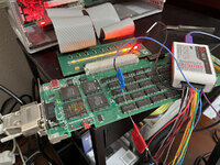
IMG_8230.JPG

May need to get that clip... getting super tedious attaching and detaching probes. 🤪 but the ability to run the card lying flat outside of the case has been super helpful.

(note: the crazy bodge wiring near the video connector is unrelated to the issue - it's a hack to disable the sync signals on the RGB channels so that my LCD doesn't have washed out colors - I have a jumper to turn the sync signals on/off)
 

MacOSMonkey

Well-known member
Sounds like you are very close to the solution now. There could be via/pad fractures from impact or something hanging on the lines -- check the caps -- (and check any package fractures as you did before). Also, check SMT02 carefully.

Definitely consider a chip clip - would be perfect for your pod and save you a lot of time. Just make sure you get one with the correct pin spacing. The MT42C4256 package pin-spacing is: 50 mil/1.27mm 28-pin SOJ.

It looks like the one you want is the Pomona 5437 - DigiKey may be cheapest ($35.19)

Mouser is similar ($35.69):

There are no better results from my favorite aggregator sites: octopart.com, findchips.com

Watch out for ebay scammers who sell clips for a cheap price and charge $25 in shipping. However, you may be able to get a Pomona clip set cheaply that would cover a range of devices -- might be worth it for the future.
 

jmacz

Well-known member
Argh... the last note regarding the 3 CAS lines being faulty is wrong. I forgot to increment a value (the frame buffer address) for the other 3 CAS line tests and thus those lines are working. Need to retest full read/write cycles on those other chips again. 😭
 

jmacz

Well-known member
With my logic analyzer probes connected, and plotting pixels via 'move' instructions, I have been looking at the various RAS/CAS/WE signals and as far as I can tell, the VRAM operations seem to be working properly. The 3 RAS signals and 4 CAS signals look ok.

BUT there's something weird going on. Again, requests to fill in pure black or pure white are not fully correct but close enough where I get a near black/white screen. With that in mind:

I've got a near black screen. (I filled the frame buffer with zeros). Here's the results of reading the first 8 pixels from the frame buffer:

Code:
 Displaying memory from e0100000
  E0100000  0000 8086 0000 0006  0000 0006 0000 0006  ¥¥¥¥¥¥¥¥¥¥¥¥¥¥¥¥
  E0100010  0000 0086 0000 0006  0000 0006 0000 0006  ¥¥¥¥¥¥¥¥¥¥¥¥¥¥¥¥

There are eight 32 bit values there (representing the 8 pixels). Each pixel is **RRGGBB (the first byte I'm ignoring as @MacOSMonkey mentioned it's ignored/unused -- and it's always zero, no issue with that one as it's not stored, it's fixed to zero). As you can see, it's not totally black as although I filled the memory with zeros, you see 0x00008086 (which should be a cyan color but my screen is black -- and again, the output to monitor path is working correctly). There are also 0x00000006 (which is close enough to black where my naked eye wouldn't be able to tell) but still not the zeros I sent.

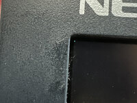
Now I issue a write to the very first pixel and the assembly instruction was to fill those 32 bits with 0x00224466. My logic analyzer was set to trigger on the WE (write enable) signal and it triggers. The logic analyzer shows the memory address lines were properly set for that particular pixel, and the RAS/CAS looks good. Here's a screenshot of the monitor:

IMG_8245.JPG

You see one pixel lit. It has a color that's approximately correct for an RGB value of 224466 (should be a cyan). And here's a dump of the frame buffer memory at this point:

Code:
 Displaying memory from e0100000
  E0100000  00A2 C4E6 0000 0006  0000 0006 0000 0006  ¥"@f¥¥¥¥¥¥¥¥¥¥¥¥
  E0100010  0000 0086 0000 0006  0000 0006 0000 0006  ¥¥¥¥¥¥¥¥¥¥¥¥¥¥¥¥

You can see it did not write the 0x00224466 I had requested .. there was some bit corruption and it wrote 0x00a2c4e6 instead. The high 4 bits in each color (RGB) were corrupted. The other 7 frame buffer bytes remain as they were previously.

My logic analyzer is set to trigger on a WE again. And I'm dumping various addresses in the frame buffer when I see this for the same frame buffer memory I was dumping before:

Code:
 Displaying memory from e0100000
  E0100000  0022 C0E6 0000 0006  0000 0006 0000 0006  ¥"@f¥¥¥¥¥¥¥¥¥¥¥¥
  E0100010  0000 0086 0000 0006  0000 0006 0000 0006  ¥¥¥¥¥¥¥¥¥¥¥¥¥¥¥¥

Huh? The memory changed (in red). My logic analyzer did NOT trigger so the WE never happened. No write instruction happened to the VRAM yet the value has clearly changed. What the heck??

Now I issue a write to the second pixel and the assembly instruction was to fill those next 32 bits with 0x00113355. My logic analyzer again i set to trigger on the WE signal and it triggers. There was only ONE write in my logic analyzer buffer (2 seconds) and it's for the pixel I requested, and again the memory address lines, RAS/CAS, all look good. Here's a screenshot of the monitor:

IMG_8247.JPG

You see the second pixel is now lit. It has a color that's approximately correct for an RGB value of 113355 (should again be a cyan). And here's a dump of the frame buffer memory now:

Code:
 Displaying memory from e0100000
  E0100000  00A2 C0E6 0011 3357  0011 3357 0011 3357  ¥3sw¥¥3W¥¥3W¥¥3W
  E0100010  0011 3357 0000 0006  0000 0006 0000 0006  ¥¥¥¥¥¥¥¥¥¥¥¥¥¥¥¥

Huh? The request I made (pixel two -- second set of 32 bits) is almost correct but there was bit corruption in the lower 4 bits of blue. The previous pixel changed values again (the first set of 32 bits). But look at pixels three, four, and five. It has copies of the bad write to the second pixel! I didn't ask for those writes. My logic analyzer shows only a single write happened. And as I start dumping some of the frame buffer memory, the values change again slightly (again my logic analyzer says nothing is happening on the VRAM side):

Code:
 Displaying memory from e0100000
  E0100000  0033 F3F7 0011 3357  0011 3357 0011 3357  ¥3sw¥¥3W¥¥3W¥¥3W
  E0100010  0011 3357 0000 0006  0000 0006 0000 0006  ¥¥¥¥¥¥¥¥¥¥¥¥¥¥¥¥

And my monitor still shows only 2 pixels lit during this time. If that memory dump was correct, I should be seeing a 3rd, 4th, and 5th cyan pixel but nope, there are only two.

What this seems to suggest is that the VRAM side is actually ok. But read operations are getting corrupted before it gets back to the computer from the video card. All the VRAM operations are happening via the SMT-02S so I think the VRAM side of the SMT-02S is ok (as far as I can tell). But what is returned from the SMT-02S back to the computer is getting garbled? I need to look at that path some more and given the physical damage happened to the Nubus connector (although again, I am finding no shorts between any pins based on resistance values).
 
Top