I thought about that when I first looked at the datasheet for the ENC624J600 - it has a built-in cryptographic offload engine, but a) I suspect that's probably biting off a bit more than I could chew, b) it seems to be a moderate pain to actually use, and c) looking at the errata, a big chunk of it is actually unusably broken. So much for that idea.Oh yes, A/ROSE is one of those "so far ahead of its time" ideas. I'ver always fancied the idea of building a smart NIC for Macs possibly using A/ROSE with TLS offload, or something - but I'm not competent to. So. One can dream.")
-
Updated 2023-07-12: Hello, Guest! Welcome back, and be sure to check out this follow-up post about our outage a week or so ago.
You are using an out of date browser. It may not display this or other websites correctly.
You should upgrade or use an alternative browser.
You should upgrade or use an alternative browser.
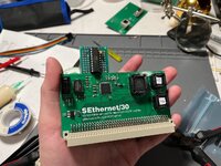
SEthernet and SEthernet/30: A new take on PDS Ethernet
- Thread starter halkyardo
- Start date
eharmon
Well-known member
Fun fact: after I probed around, it seems the final MCP Ethernet NB driver.......completely bypassed A/ROSE and ran the Sonic chip directly. And from my basic benchmarks, it's faster than the earlier drivers.
So yeah, A/ROSE is neat but not likely to add a lot of value here I suspect. At least, not without a lot of effort. It's possible using the older A/ROSE drivers might work if you implement the A/ROSE message protocol on the card. IIRC, the drivers work by running an A/ROSE application instance on the main system which uses its custom IPC to speak to the A/ROSE application on the card. Instead of running A/ROSE on the card you could just speak the same protocol. But it's unclear that would result in anything faster or better than a period NuBus card.
That said, I have imagined a card which runs A/ROSE on an FPGA with an insanely clocked 68000 core to offload TLS...
Had a quick look yesterday's evening, and it turns out that routing space is quite full - the pass-through connector & FPU have a lot of signals. i might be able to squeeze the components in there, but routing will be ugly :-/ Might go for a dedicated board & a dual-slot adapter... though signal integrity-wise, that might be more of a problem.Please do!
Anyway it brought up some questions:
(a) one of curiosity; the magnetics are on the main board & the connector on the breakout; is that a requirement signal-wise? I usually use a RJ45 connector with embedded magnetics and LEDs to save on space and complexity...
(b) SPISEL is pulled up (it's also /INT); however, that will select SPI mode rather than parallel mode - shouldn't it be pulled low? (which requires it to not be directly connected to the Mac's IRQs that are active-low!).
(c) I don't understand the (probably WiP) programming of the GAL w.r.t DSACK, see below
When reading from the '020/'030 (and I suspect the '000 is similar), the data are latched by the processor at the falling edge following the assertion of DSACK. To ensure this works, there's a timing requirements #31 on "DSACK» Asserted to Data-In Valid", which is 50ns @ 16 MHz for the '020 (43/28 at 20/25 for the '030). However, for the ENC424J600, the timing is "TPSP2 RD, EN, BxSEL to Data Valid — — 75 ns [min/typ/max]".
I don't see how that's achievable with just combinatorial GALs. BxSEL will be driven one GAL delay after ETH_CS, which is fine, but then the chip will take up to 75ns to put the correct data on the bus after that. That's too slow for any '020/'030, even if that's probably fine for a 8 Mhz 68000 (
(a) one of curiosity; the magnetics are on the main board & the connector on the breakout; is that a requirement signal-wise? I usually use a RJ45 connector with embedded magnetics and LEDs to save on space and complexity...
All the vertical integrated jacks I could find looked like they were going to be a tight fit through the case opening, so I thought I'd play it safe and go for separate magnetics. As far as putting them on the main board vs. the breakout... mostly an arbitrary decision. Either way, taking the signals off-board before or after the magnetics goes against all the ethernet layout best practices that I can find, and possibly the ethernet spec itself.
Having the magnetics on the main board might help deal with any common-mode noise picked up by the cable to the breakout board, but I suspect it's probably not significant enough to really worry about. Having said that, all the PDS ethernet cards I've examined have common-mode chokes on their internal AUI connection to the breakout board.
(b) SPISEL is pulled up (it's also /INT); however, that will select SPI mode rather than parallel mode - shouldn't it be pulled low? (which requires it to not be directly connected to the Mac's IRQs that are active-low!).
All I can really say about that is "oops!" The perils of doing all this stuff late at night when I'm tired.
The ENC24J600's interrupt output is push-pull (except during power-on where it's read as SPISEL), so if it's weakly pulled down it's still usable as an interrupt pin, but that was a rather silly mistake!
Yeah. I just came to that realisation last night and was just about to come here and admit to my screw-up(c) I don't understand the (probably WiP) programming of the GAL w.r.t DSACK, see below
When reading from the '020/'030 (and I suspect the '000 is similar), the data are latched by the processor at the falling edge following the assertion of DSACK. To ensure this works, there's a timing requirements #31 on "DSACK» Asserted to Data-In Valid", which is 50ns @ 16 MHz for the '020 (43/28 at 20/25 for the '030). However, for the ENC424J600, the timing is "TPSP2 RD, EN, BxSEL to Data Valid — — 75 ns [min/typ/max]".
I don't see how that's achievable with just combinatorial GALs. BxSEL will be driven one GAL delay after ETH_CS, which is fine, but then the chip will take up to 75ns to put the correct data on the bus after that. That's too slow for any '020/'030, even if that's probably fine for a 8 Mhz 68000 (where the similar #31 "DTACK Asserted to Data-In Valid" is 90nssee below). So for me, DSACK has to be delayed somehow, rather than the current combinatorial I see in the code. As the ENC424J600 doesn't have a 'data ready' signal (which would have made everyone's life easier!), that probably means waiting for a number of clock cycles, such as from the CLKOUT signal of the ENC424J600 (as the CPU clock my vary depending on the specific Mac and presence of an overclock or accelerator).
 . I'd somehow completely missed the read timings in the datasheet, and was only going by the write timings, which looked to be quick enough that I could just assert DSACK combinatorially and assume that the data would be ready by the time it was sampled. Looking at the timing specs for the flash part I'm using for the declaration ROM, I probably have the same problem there, or at least cutting the timings way too close for comfort.
I don't have enough space to implement a wait-state generator on the existing GALs, so I'm a bit stuck there. Might be able to add a 'bodge board' with a counter feeding a free input in U4 to delay DSACK, but it'll be a very ugly bodge indeed. Once again, the perils of sleep deprivation. Though Microchip's choice to put the timing diagram and the actual timing numbers 100 pages apart definitely didn't help!
I'm already working on moving everything into a CPLD for the next revision (chose the ATF1502 just because it's cheap and 5V and my GAL tools support it). Might make the wait-state cycle count configurable by jumper to allow for faster machines - I've been looking at the IIfx PDS too, and while I already have a NuBus ethernet card in mine, I think that so long as the logic can keep up with the faster clock, it should theoretically work in that as well!
Yep, that's right. Couldn't quite believe it, but I double-checked on my SE and indeed, without anything in the PDS slot I can happily read garbage from empty spaces in the memory map without taking a bus error... speaking of the 68000, I don't see a connection to DTACK on the SE version? Isn't DTACK required to be asserted by devices?I see in the readme you delegate that to the BBU, which will also take care of the timing on the SE.
If an SE PDS device does need wait states, it can assert /EXT.DTK to tristate the BBU's DTACK output, but I'm pretty sure that at 8MHz the ENC624J600 is fast enough to not need it, even taking the GAL delay into account.
Last edited:
OK, make sense. Those openings are small and not super convenient - couldn't find a way to properly fit the HDMI connector either :-( I gave up on the (IIsi|Quadra)FPGA by having them completely inside the case. I was thinking of doing the same with ethernet, but then I figured if you're going to validate the design... might want to leverage that as wellAll the vertical integrated jacks I could find looked like they were going to be a tight fit through the case opening
If I want to stack the design in a secondary PDS on an adapter, the board needs to be quite small as the IIsiFPGA is very thick with the stacked FPGA board. That's why I'm thinking SMD CPLD rather than through-hole, and probably no ROM for similar reason- the DeclRom for Ethernet can live in the IIsiFPGA if they're intended as a combo. Your board looks good but is too tall for my use case.
So question - for the board-ot-breakout connector, the name on the schematics is 2x05, the actual schematics is a 2x04 pins and so is the footprint, while the part number seems to also be for a 2x05... I'm guessing you're planning on 2x04 and the part number is a leftover (probably from the VGA on the breakout, which is a 2x05!), do you have a part number for that? And also, do you plan on a custom cable or do you have a part number for the cable w/ connector as well?
From the latest update in the Git, seems that's how you decided to goI don't have enough space to implement a wait-state generator on the existing GALs, so I'm a bit stuck there. Might be able to add a 'bodge board' with a counter feeding a free input in U4 to delay DSACK
... does it mean you have something already sort-of-working in the SE/30 ? Or is that still theoretical at this point?
Yes, "Guide to the Macintosh® Family Hardware (2n Ed)" p126 (PDF p165) for those intrigued.:Yep, that's right. Couldn't quite believe it, but I double-checked on my SE and indeed, without anything in the PDS slot I can happily read garbage from empty spaces in the memory map without taking a bus error.
I was also surprised, but do not have the relevant system(s) to test. I can assure you on the '030 and '040 PDS, you need to answer the CPU or you take a bus errorWith two exceptions - noted in the next paragraph - the BBU always generates either
/DTACK or /VPA in response to a memory access, even to an address space with no
device (...)
So question - for the board-ot-breakout connector, the name on the schematics is 2x05, the actual schematics is a 2x04 pins and so is the footprint, while the part number seems to also be for a 2x05... I'm guessing you're planning on 2x04 and the part number is a leftover (probably from the VGA on the breakout, which is a 2x05!), do you have a part number for that? And also, do you plan on a custom cable or do you have a part number for the cable w/ connector as well?
I'd originally planned on a 10 pin connector to the breakout board just because I had some 10-pin cables lying around from another project, but when I realised that my video card's connector is also 10-pin, I thought that maybe I should make them different
.At least for the prototypes I'm just using flat ribbon cables with 2.54mm IDC connectors. Might not be the best for signal integrity but it'll probably work well enough.
Still theoretical, but I've been simulating it and I'm pretty sure it'll do the job. Hopefully the boards will arrive this week and I can test my theories. I'm already planning out another revision using a small CPLD as I probably should have done to begin with.From the latest update in the Git, seems that's how you decided to go
... does it mean you have something already sort-of-working in the SE/30 ? Or is that still theoretical at this point?
Even before getting the boards, I think we can consider this first attempt to be 'educational' - if it doesn't work, I'll try again with the CPLD-based design. If it works, it'll at least prove the concept and let me start working on the driver, but the CPLD-based design is probably a better way to go for actual production anyway.
Bolle
Well-known member
It will be fine.At least for the prototypes I'm just using flat ribbon cables with 2.54mm IDC connectors. Might not be the best for signal integrity but it'll probably work well enough.
Magnetics should be placed on the main card just the way you did and not on the breakout board.
Source: been there and tried both. Magnetics on the main card is way more robust when it comes to the quality and/or length of the IDC cable.
With minimal cable length and good thick wires it's fine either way. I ended up making my own cables.
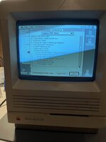
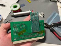
The boards and parts arrived this weekend, and we have some signs of life! Managed to bodge around my timing bug on the SE/30 board in an ugly but workable fashion (that gigantic solder glob on R2 is another bodge. I may be bad at SMD soldering but I'm not THAT bad!)
The declaration ROM shows up exactly as it should, and I'm able to fire up Macsbug and read and write the ENC624J600's registers without a problem, but its buffer RAM is another matter... whether I'm accessing it directly, or indirectly through chip registers, it doesn't seem to behave - anything that I write comes back scrambled, like I've got address lines shorted, except those same address lines can happily access the registers. I've relaxed the /DSACK delay all the way out to 8 cycles/500ns (confirmed on my oscilloscope) so I don't *think* it's a timing issue, starting to wonder if I killed the chip somehow.
Still, I'll call this a win. The basic design seems to be viable, I've learned a few more things for the next revision, and if it comes to it, I've got a spare ENC624J600 to swap out. Onward!
Attachments
Hopefully you will figure it out. My first instinct was a timing issue (different behavior between registers and SRAM in practice), but if indirect accesses through registers are affected it can't be that...The declaration ROM shows up exactly as it should, and I'm able to fire up Macsbug and read and write the ENC624J600's registers without a problem, but its buffer RAM is another matter... whether I'm accessing it directly, or indirectly through chip registers, it doesn't seem to behave -
The fact you can talk to the ROM and the registers is definitely a win
Turns out the ENC624J600 doesn't like its byte-selects being wiggled when its chip-selects aren't asserted - previously I'd just been decoding them based on access size and A0, and assumed it would ignore them when it wasn't selected. But when I gated them behind the chip select, it started working!Hopefully you will figure it out. My first instinct was a timing issue (different behavior between registers and SRAM in practice), but if indirect accesses through registers are affected it can't be that...
The fact you can talk to the ROM and the registers is definitely a win
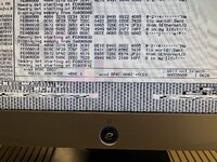
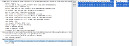
Just managed to send my first packet down the wire by poking at it through MacsBug, which was immensely satisfying. Now to go insane staring at Inside Macintosh until I can get my driver to work

I also figured out a more elegant solution for generating the various delays required by the ENC624J600, independently of the system's clock speed. It has an software-configurable clock output that defaults to 4MHz, but when set to 25MHz, all my delays become convenient multiples of the clock period, with a couple of nanoseconds of safety margin. It won't be synchronous with the CPU clock of course, but I'm pretty sure that my delay logic (up-counters that are held in reset until their start condition) should be OK for that. No jumpers required, and if it turns out that my timing was too aggressive, the clock can just be scaled back in software.
Also it turns out that with that clock modification, it works perfectly in my IIfx's PDS slot as well, which is extremely convenient because it's a lot easier than digging inside the guts of a Compact Mac when I need to reprogram a GAL or put the scope on it! I threw together a crude memory benchmark, and in the IIfx, I can read and write to the packet buffer at a bit above 20MByte/s. I'm sure that the network stack will keep real-world speeds well below this, but it bodes well for theoretical performance exceeding the 10Mbit barrier.
I'm properly pleased!
Attachments
Congratulations! That's a huge result!Just managed to send my first packet down the wire by poking at it through MacsBug, which was immensely satisfying. Now to go insane staring at Inside Macintosh until I can get my driver to work
I hadn't realized CLKOUT defaulted to 4 MHz. That means your timings must 'work' (even slowly) at 4 MHz so that the CPU can reprogram COCON to generate the 25 MHz clock, I suppose? Annoying chicken-and-egg problemIt has an software-configurable clock output that defaults to 4MHz, but when set to 25MHz
The IIfx PDS will run at an apparent 20 MHz when using a pseudo-slot device in $E. It's a weird design.Also it turns out that with that clock modification, it works perfectly in my IIfx's PDS slot as well
Theoretically, you can alternatively use $7 ("fast slot space area") to get all the signals at 'native' speed of 40 MHz. I don't know of any design doing that, one of the reason being the IIfx doesn't expose it's 40 MHz clock, only the 20 MHz one... But your design currently doesn't need the CPU clock. So you might be able to try 40 MHz bus operation to see if it improves performance (assuming you can improve timings a bit, perhaps pusing CLKOUT to 33 MHz to get finer tuning).
Downside is, $7 is not enumerated by the Slot Manager. So either the driver need to trust the hardware is here, or you could just have a DeclRom in $E declaring a device in $7.
An so you should beI'm properly pleased!
cheesestraws
Well-known member
Just managed to send my first packet down the wire by poking at it through MacsBug, which was immensely satisfying. Now to go insane staring at Inside Macintosh until I can get my driver to work
Very, very well done. :-D This is really cool.
Thanks! Don't put too much stock in what I have to say, at least until I get the whole thing working!Congrats! That's so cool to see the packet, what a great feeling. I want to say I really appreciate all the documentation and explanations you've put in your source code. For someone with only software knowledge, it's been quite enlightening.

The commenting might be a little bit on the excessive side but I find that it helps a lot in the process of wrapping my head around what's going on. I'd like to turn it into a more structured writeup some day, but I'm not a Websites Person and the idea of setting up a blog is actually kind of intimidating to me!
I just realised that I'd forgotten to push the last few day's worth of changes up to Github, so there's a little bit more to peruse there (mostly just some refactoring, plus my quick 'n dirty memory test/benchmark tool).
It seems to work well enough; it's stable at 4MHz (with a whopping 500ns DSACK delay), and there's a noticeable speedup when I bump it up to 25MHz for the optimal 80ns delay. The scope trace in my previous post shows the ENC624J600's chip select on the top, and my wait-state output on the bottom (high = suppress /DSACK, low = enable /DSACK). Haven't seen any glitches.I hadn't realized CLKOUT defaulted to 4 MHz. That means your timings must 'work' (even slowly) at 4 MHz so that the CPU can reprogram COCON to generate the 25 MHz clock, I suppose? Annoying chicken-and-egg problem
Huh, interesting! The IIfx was really an incidental target since I had the machine lying around and realised that it'd be a lot less hassle to get to the card than in the SE/30. I'd read up on the 20MHz pseudoslot-$E operation, but I hadn't thought about fast slot space at all. I'm not stranger to the 'slow the CPU down for different address spaces' trick though - my last couple of hardware projects have been for the 8-bit BBC/Acorn systems, which employ that strategy in a brute-force way by stretching the CPU clock! Makes for all sorts of fun dealing with the timing ambiguities and control-line glitches that result from it.The IIfx PDS will run at an apparent 20 MHz when using a pseudo-slot device in $E. It's a weird design.
Theoretically, you can alternatively use $7 ("fast slot space area") to get all the signals at 'native' speed of 40 MHz. I don't know of any design doing that, one of the reason being the IIfx doesn't expose it's 40 MHz clock, only the 20 MHz one... But your design currently doesn't need the CPU clock. So you might be able to try 40 MHz bus operation to see if it improves performance (assuming you can improve timings a bit, perhaps pusing CLKOUT to 33 MHz to get finer tuning).
Downside is, $7 is not enumerated by the Slot Manager. So either the driver need to trust the hardware is here, or you could just have a DeclRom in $E declaring a device in $7.
I think with the ENC624J600's timing requirements (75ns from selection to data-ready on read, must remain unselected for 40ns after a write), it's probably not going to see much benefit from going any faster, but it has got me thinking about how to optimize things in the next CPLD-based revision where I'll have more gates to play with. Right now I'm delaying /DSACK by 80ns for all accesses, but that could be skipped for writes. Much to think about.
It'll be very interesting to compare actual ethernet performance with my NuBus ethernet card, too. I wonder what a good test methodology would be; I found an early predecessor to iperf that can build and run under A/UX, but most people would probably be more interested in performance on Mac OS. I'm sure there must be some network-benchmark tools out there, anyone aware of any?
I might also have to recruit some SE/30 owners with other ethernet cards to compare against!
An so you should be
That's incredibly encouraging to hear that from both of you! Your hardware projects and writeups have been inspirational and informative and I certainly don't think I'd have been brave enough to embark on this project without having seen what you've done.Very, very well done. :-D This is really cool.
Also, just to add, I haven't forgotten about the SE board either! My SE suffered a very unfortunately-timed hard disk failure last week and it's out of commission until I get a drive emulator for it.
CC_333
Well-known member
This is a fun project!Also it turns out that with that clock modification, it works perfectly in my IIfx's PDS slot as well
If I'm not mistaken, almost no one developed anything for the IIfx PDS slot, yes?
c
I'm certainly not aware of any cards for it!This is a fun project!
If I'm not mistaken, almost no one developed anything for the IIfx PDS slot, yes?
c
For 'pseudo-slot' cards that occupy NuBus slot space and don't do anything exotic, it's mostly compatible with the 030 PDS slot in the SE/30 and IIsi - the only major differences are that it's addressed as slot $E instead of $9-$B, clocked slightly faster (20MHz, half CPU speed for Slot $E accesses), and the clock pins are used differently (CPUCLK is unconnected, and C16M is the 20MHz CPUCLK/2 signal rather than 16MHz).
Any card that can be configured for slot $E should stand a good chance of working, so long as it doesn't depend on CPUCLK or try to do anything clever like bus mastering or responding to addresses outside of slot space.
Unfortunately, the SE/30 and IIsi use $E for their onboard video so it may not be a common option, but I know that at least the Asante MacCon that Bolle reverse-engineered (which was my jumping-off point for this project) has a jumper setting for it.
The other constraints are mechanical, of course - a standard-sized SE/30 card is too tall to fit with the lid closed, and the IIfx has no provision for the remote-mounted breakout panel. I've got my breakout panel hanging out of the second floppy drive opening!
In theory the IIfx PDS slot could provide a lot more bus bandwidth than NuBus - in slot-$E mode it's clocked at twice the speed (20MHz as opposed to 10), and as Melkhior mentioned, there's another mode that allows it to operate at the full 40MHz. Especially these days with faster peripherals being commonplace, there could be quite a few fun projects to be had with it!
Last edited:
Andy
Well-known member
Congrats on getting a mention in Hackaday!
 hackaday.com
Affordable Networking For Your Classic Mac
The Mac SE and in particular the Mac SE/30 number among the more sought-after of the classic all-in-one Apple computers, and consequently their peripherals including network cards are also hard to …
cheesestraws
Well-known member
I'm certainly not aware of any cards for it!
(Parenthetically, and without meaning to derail your thread: there was at least one SCSI card for it, the SCSI Bolt, by a company confusingly Sixty Eight Thousand. They also made an even rarer 040 PDS version.)
Similar threads
- Replies
- 4
- Views
- 293