• Updated 2023-07-12: Hello, Guest! Welcome back, and be sure to check out this follow-up post about our outage a week or so ago.

Quadra 840av ROM SIMM?

dougg3

Well-known member
I've been playing with various ROM hacking stuff on the II series Macs, and I found this on eBay and couldn't resist snatching it up. It's a really weird shape!

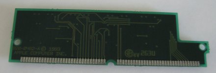
AVSIMMTOP.JPG

AVSIMMBOTTOM.JPG

Googling for the part number 820-0482-A seems to find a few results implying it's a 64-pin ROM SIMM belonging to a Quadra 840av. Further Googling is showing that some (few?) 840av models have the SIMM socket, but others (most?) have soldered ROM. I have an 840av, but haven't had a chance to check if mine has the ROM SIMM socket (and if there are clearance issues explaining why the SIMM is such an odd shape). Also, since the 660av and 840av share the same ROM, it might be for a 660av instead.

Can anybody confirm that this is for an 840av? I'm tempted to figure out a way to dump the contents to see for sure. I wonder if it is identical to the ROM version that is soldered on with later models?

I've been using a continuity tester and the JEDEC standard for 32-pin PLCC chips to figure out its pinout. The pinout is ALMOST identical to the II series ROM SIMM pinout, except the chip enable line on the four chips is directly connected to GROUND (always active) on this SIMM, and the SIMM pin that was used for chip enable on the II series is now another VCC pin.


dougg3

Well-known member
Thanks! Good to know. I checked my 840av and it has the pads for the SIMM socket, but there is not actually a socket mounted on the board. It was manufactured February 19, 1994, so I'm guessing your 840av's date is going to be closer to the original date when they first started making them...


dougg3

Well-known member
For some closure on this question from long ago, I stuck the SIMM into my SIMM programmer board. I changed the firmware slightly on my programmer board to leave the CS pin as an input because it's wired differently on this SIMM than on the other II-series ROM SIMMs. Then I dumped the contents of the chips...

It's exactly the same ROM that is on my 840av's soldered motherboard ROM -- checksum $5BF10FD1. So I didn't discover any exciting lost ROM versions or anything like that. :-( Oh well! Mystery solved.


olePigeon

Well-known member
Could you solder a socket onto the motherboard and override the onboard ROM like on a IIci? Maybe a secret jumper some place? :)


dougg3

Well-known member
Ya know, I'm not sure on that! I can definitely solder a socket onto the motherboard, but I don't know what it takes to make it work. My SIMM would need a hardware mod at the very least.

The Quadra 700 is able to detect that a ROM SIMM is inserted and automatically disables the onboard ROM. My uneducated guess is that it uses one of the VCC pins on the SIMM to override a weak pull-down resistor on the soldered ROM chip select or output enable lines (thus pulling it high and inactive), but I don't know. I suppose I could check the 840av's motherboard out and trace some things, but it's such a pain to get the motherboard out that I probably won't be working on that anytime soon :) I've already broken the clips that hold the CD bezel on (such brittle plastic!)...grrrr....


dougg3

Well-known member
Just updating this post with the full pinout and physical measurements in case this helps anyone in the future who needs to make one of these or something...

SIMM pins (left to right):

Code:
 1 - VCC (+5V)
2 - not connected (A0)
3 - not connected (A1)
4 - A2 (connected to all chips' A0)
5 - A3 (connected to all chips' A1)
6 - A4 (connected to all chips' A2)
7 - A5 (connected to all chips' A3)
8 - A6 (connected to all chips' A4)
9 - A7 (connected to all chips' A5)
10 - GND
11 - VCC (+5V)
12 - !OE (connected to all chips' !OE)
13 - VCC (+5V)
14 - D0 (connected to UI's D0)
15 - D1 (connected to UI's D1)
16 - D2 (connected to UI's D2)
17 - D3 (connected to UI's D3)
18 - D4 (connected to UI's D4)
19 - D5 (connected to UI's D5)
20 - D6 (connected to UI's D6)
21 - D7 (connected to UI's D7)
22 - D8 (connected to U2's D0)
23 - D9 (connected to U2's D1)
24 - D10 (connected to U2's D2)
25 - D11 (connected to U2's D3)
26 - D12 (connected to U2's D4)
27 - D13 (connected to U2's D5)
28 - D14 (connected to U2's D6)
29 - D15 (connected to U2's D7)
30 - GND
31 - A8 (connected to all chips' A6)
32 - A9 (connected to all chips' A7)
33 - A10 (connected to all chips' A8)
34 - A11 (connected to all chips' A9)
35 - A12 (connected to all chips' A10)
36 - A13 (connected to all chips' A11)
37 - A14 (connected to all chips' A12)
38 - A15 (connected to all chips' A13)
39 - A16 (connected to all chips' A14)
40 - A17 (connected to all chips' A15)
41 - A18 (connected to all chips' A16)
42 - A19 (connected to all chips' A17)
43 - A20 (connected to all chips' A18)
44 - not connected (probably reserved as A21)
45 - not connected (probably reserved as A22)
46 - VCC (+5V)
47 - D16 (connected to U3's D0)
48 - D17 (connected to U3's D1)
49 - D18 (connected to U3's D2)
50 - D19 (connected to U3's D3)
51 - D20 (connected to U3's D4)
52 - D21 (connected to U3's D5)
53 - D22 (connected to U3's D6)
54 - D23 (connected to U3's D7)
55 - D24 (connected to U4's D0)
56 - D25 (connected to U4's D1)
57 - D26 (connected to U4's D2)
58 - D27 (connected to U4's D3)
59 - D28 (connected to U4's D4)
60 - D29 (connected to U4's D5)
61 - D30 (connected to U4's D6)
62 - D31 (connected to U4's D7)
63 - VCC (+5V)
64 - GND
Pinouts of each PLCC chip:

Code:
 1 - labeled as A18 by JEDEC, but it's connected to VCC on the SIMM -- possibly !WE on earlier standard
2 - A16
3 - A15
4 - A12
5 - A7
6 - A6
7 - A5
8 - A4
9 - A3
10 - A2
11 - A1
12 - A0
13 - D0
14 - D1
15 - D2
16 - GND
17 - D3
18 - D4
19 - D5
20 - D6
21 - D7
22 - labeled as "!CE" by JEDEC. SIMM connects it directly to GND so it's always active.
23 - A10
24 - !OE
25 - A11
26 - A9
27 - A8
28 - A13
29 - A14
30 - A17
31 - labeled as !WE by JEDEC, but it appears to be used as A18 on the ROM chips. maybe different standard.
32 - VCC (+5V)
Size:

Dimensions are pretty much the same as my 8 MB ROM SIMM (see the EAGLE file at http://code.google.com/p/mac-rom-simm-programmer/), except there's a cutout in the upper left corner. The cutout begins 81.5 mm from the right side of the SIMM, and it begins 13.6 mm from the bottom of the SIMM.

Other notes:

It's exactly the same as the earlier SE/30 and II series ROM SIMM pinout, but with these exceptions:

  • The chips don't pay attention to the older pinout's !CE pin -- the chip enable pins on the four chips are wired to ground so chip enable is always active.
  • The older pinout's !CE pin is wired directly to +5V.


Chip markings are as follows:

U1 = 341S1078

U2 = 341S1079

U3 = 341S1080

U4 = 341S1081

Sticker on SIMM says 341-0675

PCB silkscreen says 820-0482-A

APPLE COMPUTER INC.

PCB, 2 MEG SIMM © 1993


dougg3

Well-known member
One minor correction, I was reading the JEDEC standard for 512K x 8 single-supply EEPROM and I should have been reading the JEDEC standard for 512K x 8 EPROM. On the actual PLCC chips, pin 1 is VPP (so supplying 5V probably means don't go into programming mode) and pin 31 is indeed A18. So that removes the two concerns I had about the wiring of the PLCC chips themselves.


mcdermd

Well-known member
I think I have a few random, stock Apple 840av ROMs that came with a really odd assortment of stuff if they would help anyone.

 
Top