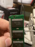
Cleaning up a bombed SE/30 and there was enough gunk on the ROM that I took it apart to clean it. (As well as ordering a new simm socket for it.)
I damaged/tore one (1) solder pad on it, which is actually good for me, and I can bodge it easily enough but can’t figure out where it’s supposed to go. The corresponding pins on the other chips don’t seem to connect to anything (no connectivity to any pins, grounds, other components, etc.) and when I had the chips off, I couldn’t see a trace coming off of the missing pad.
Anybody know where this pin is supposed to go? (Upper right of photo, I guess pin 1?)

 .. sorry