Salvaging bombed SE/30 ROM lines A(8) A(9) shorted?!

ironborn65

Well-known member
My conquest here
is being salvaged.. at least I'm trying to.

I removed the obvious destroyed chips: RTC, D1, D2 (caps are the easy thing) and the RAM muxes UJ1, UJ2, UJ3.
I'm now looking for continuity, the traces from the muxes to the ROM SIMM.
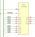
The inputs are in pairs, e.g.: for UI2, A(7) in 2,5, A(9) in 11,14, A(6) in 3,6, A(8) 10, 13. ...

But I was surprised to notice that A(9) and A(8) are shorted, i.e. pins 31 and 32 in the ROM SIMM.
For the other muxes, there are no shorts in the corresponding lines.
After some thorough checking, I decided that "The mux is shorted" so I desoldered it but "what?", it's still shorted!

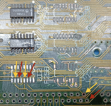
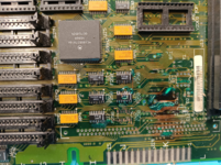
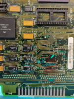
In the picture below(*) IMHO red and yellow arrows are supposed to be separated but they are instead shorted.
Does it make sense?

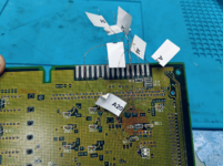
The PCB was cleaned in vinegar, IPA, dishwasher and in the ultrasonic cleaner.

(*) yes, traces and pads are not in good shape, but at least I'll improve my soldering skills and the schematics of the SE/30.


1728423652229.png
View attachment 79401
1728425545090.png
 

ironborn65

Well-known member
I checked another working SE/30 board and the two traces are - obviously - not shorted.
I was expected to repair missing connections, not to remove new ones :)
There is a short somewhere, which can be more tricky, maybe inside the layers??? How could it happen? The red trace goes inside a via, and the yellow one straight to the pin. I might never find and remove the bridge. I could drill a larger hole in pin 32 ROM SIMM hoping to break the connection and add a bodge wire from the back side to the mux.
Is there any experience about "new" connections, or bridges when fixing a bombed motherboard?

Plan B is getting closer ....
 

ironborn65

Well-known member
this is my progress on my journey and I have a question about some traces.
I have addressed the traces of the RTC section (Y1 is not required, in fact pins 2 and 3 are NC), I'm waiting for diodes and the ATTiny85 replacement.
I've added a bodge wire for the RCMUX line UJ2 UJ3 and UJ4, which is connected with the others.
I'm also waiting for the pads and trace patches

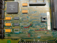
But I have a big issue approaching: there are many lines, and some have been identified in the attached photo, that come from a via and go to another one. The vias have been destroyed by the acid and they did not have contact anymore with the underlying layer. How can I add a bodge wire if I don't know either the origin or the destination? I can only think of testing for continuity ALL the traces related to PDS slot, ROM, ADDRESS, DATA and control lines. Quite an impossible task.
I don't want to use a working SE/30 because the traces need to be scraped a bit ... not a wise thing to do to a working machine.

Any suggestion ... besides going the "reloaded" path?


1728832136777.png
 

SparrowRat

Well-known member
You shouldn't need to scrape back solder mask on a working SE/30 - you could just put your meter probe on a via.
 

LaPorta

Well-known member
There may be crap in between the layers shorting the pads. Why not just ditch the pads, solder bodge wires directly to the legs, sever the traces before they reach the holes, and patch with the other end of the wire?
 

ironborn65

Well-known member
@LaPorta , thanks I'll go that way. I'll keep posted.
At the moment I'm mapping the traces
1729238976855.png
I'm worried about the Address lines splitting in the middle layer because they reach the 74F258 (MUX), the ROM SIMM, VIA2, VIA2 and the CPU/FPU. Sometimes I see traces splitting on a surface on a via, but maybe not always.
After fixing the traces from the muxes to the ROM SIMM I must check if they reach also the other destinations.
It's weird "to me" that A0 and A1 are not used in the ROM SIMM.
 

cheesestraws

Well-known member
It's weird "to me" that A0 and A1 are not used in the ROM SIMM.

you're always reading 4 bytes at a time And always aligned on a 4-byte boundary. So it doesn't matter what A0 and A1 are, because A0 increments your address by a single byte and A1 by two. Even if A0 or A1 were 1, the SIMM doesn't care and even if it could it can't respect that because it's always doing an aligned 4-byte read. So they're irrelevant.

edit: ymk beat me :)
 

ironborn65

Well-known member
I soldered 3 new MUXes at UI2, UJ4 and UJ3. UJ2 will be challenging, I'm waiting for the Spot Soldering Pad to re-create the pads.
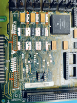
I have made a "map" to keep track of the fixes required.
I have not done the same for the data lines, they are in the area because of the ROM SIMM, I noticed the D0 and D17 are interrupted, so I need to test for all 32 traces.
UI2 and UJ4 have been soldered pretty decently, but UJ3 is a mess, I'm clumsy with bodge wires. I'm using copper from the windings of an electric motor. Maybe I should use plastic-isolated ones.
It is harder than expected and still, it's not sure if it will work.

1729461090006.png

1729460890229.png
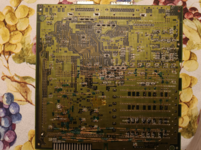
The back of the motherboard is waiting for the ROM SIMM to be installed, and then I'll wire the bodges, and they are not all of them.
1729461658450.png

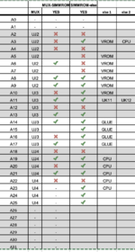
The pdf table from https://github.com/mishimasensei/macse30mlb with the connections of address and data lines is very useful. I could not find a table for the other signals, like the ROM*, that in my case is interrupted. Sure thing I can browse the schematics manually.

I'm learning to use fewer solder mask because I've noticed that it does not dry fully with the UV light if too thick.

I've successfully used conductive glue in some sections of the board to re-connect the traces and I added a layer of solder mask.

Using a reference working SE/30 motherboard is extremely useful for those interrupted traces that emerge from a VIA and get inside another one.

I have the impression from the videos and blog I see that despite the careful inspection and commitment to fixing traces, the happy chime will not happen at first boot and maybe never. The bombed macs can be subtle.
 

ironborn65

Well-known member
UJ2 is now in place, and all connections are routed as intended.

Creating the pads and traces for UJ2 was particularly challenging for me. The MUX is slightly crooked, which is a bit painful to look at, but there’s continuity and no shorts, so I’m satisfied. I didn’t think I’d manage to get this far.

Yes, my work may look quite rough, but I’m learning a lot along the way. I hope it’s sturdy enough to withstand an IPA bath when I’m finished.

It’s not complete yet—there are still broken traces to repair, and the ROM SIMM is waiting for me
1730037952695.png
 

ironborn65

Well-known member
Data and address lines are all set now... what a mess!

I managed to avoid four bodges by restoring contact from two vias to the trace. The acid had eroded the surface of the vias, breaking the connection with the trace, it went almost unnoticed. Using solder paste and quality flux, I was able to solder a thin wire inside the via and create contact with the trace by carefully bending the wire.

Now, I need to triple-check everything before starting to reattach the removed components.
Oh .. I did not care about all the lines to the PDS slot yet.


1730740804020.png
 

ironborn65

Well-known member
I'll try, tks, today I put it under the sunlight... I can dry all of it in a batch :)
 
Last edited:

ironborn65

Well-known member
I've added all the previously broken traces, to the best of my ability.

The Address and Data lines have been fixed, along with the RCMUX, GND, VCC, and all the resistor lines associated with the RAM multiplexers, plus RAAF and RABF lines to the RAM SIMMs. The PDS lines are not yet connected; I will address them once the rest of the system is operational.

Since the ROM SIMM is slightly bent, I tested continuity for all pins from the SIMM to the ROM chips on the SIMM PCB. I'm using the original stock ROM SIMM. All connections tested fine, although I discovered the ROM signal wasn't reaching the glue chip, so I added an additional bodge wire to restore this connection.

I verified there are no shorts across the V12, V5 rails, and GND, as well as on all pins where bodge wires were added. I did find and correct one bridge in this area.

The ATTiny85-based RTC module has been added, excluding the D1 diode, Y1 crystal, and capacitors C44 and C45. However, I added the D2 diode for reverse polarity protection.

With some apprehension, I powered up the system using a known working PSU. Unfortunately, it remained silent, with only the fan spinning.

The +5V lines read 4.97V, while the RTC VCC measures only 4.2V. Before the D1 diode, the voltage is 4.9V. I don't believe this minor discrepancy is enough to prevent the system from chiming.

At present, only the CPU and the video multiplexers show any warmth. I would now start with checking the boot sequence.
Any suggestion?
Where to check if the CPU is trying to do something?
 

ironborn65

Well-known member
There may be crap in between the layers shorting the pads. Why not just ditch the pads, solder bodge wires directly to the legs, sever the traces before they reach the holes, and patch with the other end of the wire?
@LaPorta ... I feel like I’m nearing the end of this journey unless I have an epiphany or receive some helpful advice here.

As described in this thread: Mac SE/30 Silent, No Startup Bong, the short appears to be in the middle layer of the PCB.

I’ve already cut the traces before they reached the via, but without success. I’m now left with a CPU section where the bodge wire goes. Unfortunately, it’s soldered into the PCB, and there are no visible traces. Additionally, the exposed vias in the area don’t correspond to either A(8) or A(9).

One option would be to drill small holes around pin A(8) or A(9), hoping to intercept the trace within the layer. However, this carries the risk of making the problem worse or potentially damaging the CPU from below.

I haven’t been able to find a PCB schematic for the original SE/30, which could guide me in performing a more precise "surgery". The logic schematic doesn’t help for this task.
 
Top