• Updated 2023-07-12: Hello, Guest! Welcome back, and be sure to check out this follow-up post about our outage a week or so ago.

LC III - Mostly dead.

Stephen_Usher

Well-known member
I've been handed an LC III which had some localised battery damage but the CPU pins got damaged and the previous owner tried to fit a new CPU, got stuck and handed me the machine.

I've replaced the CPU with another one and although it doesn't look great all the legs tone out correctly.

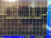
However, the CPU on power up only goes through a small number of read cycles, /BUSERR goes low for about 10ns and the CPU stops with /HALT still high.

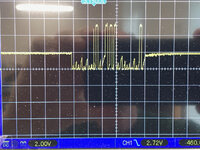
Attached is an image of the activity measured using a logic analyser.

I don't have a hex dump of the ROM so I can't see it the top nibble is correct for the first few words. (I was looking here for addresses as the beginning of the ROM reading should be giving the CPU addresses to set up the jump table, interrupt vector, stack and program counter.

Resetting the machine gives the same result.
 

Attachments

  • IMG_3637.jpeg
    IMG_3637.jpeg
    1.2 MB · Views: 18

Stephen_Usher

Well-known member
Further investigation shows that the CPU is reading the first two words of the ROM and then reads an address with the same lower nibble as the second word of ROM, which would be an instruction fetch for the ROM entry point. It then reads another word from the next address and then tries to read some other address and the system hangs until there's a bus error many, many clock cycles later.
This suggests that whatever the second instruction is trying to read from isn't responding.

Does anyone have a ROM disassembly for the LC III ROM so I can see what it's trying to access?
 

Stephen_Usher

Well-known member
I've got a little further with the diagnosis.

After replacing the HI ROM socket with a new one as the contacts on the original were corroded there was no change, but I noticed that D20 and D21 looked strange so lifted the D21 leg. This looked good when out of the socket. Checked D21 on the PDS slot with the pin lifted and there was still a signal... The same as D20.

There was a 2ohm short between the data lines. Having seen a similar short previously on this system I ran a knife blade between the D20 and D21 pins on the CPU where they enter the package... 5ohms. Another go, 20 ohms. More rubbing and the short is gone.

Has anyone else ever seen shorts on a QFP package like this where you have to essentially scratch away part of the plastic package to stop a short?
 

Stephen_Usher

Well-known member
The machine now constantly cycles crash/reset but it's inconsistent, depending upon whether D0 is high or low at the end of the sequence.

If D0 is high then the CPU quiesces for a while before restarting. If it's low then it immediately restarts.

R/W on the CPU is constantly high, as is /BERR and /HALT as far as I can see.

Does anyone have any thoughts as to what may be causing this, other than a duff CPU (which I can't rule out).
 

Attachments

  • IMG_3640.jpeg
    IMG_3640.jpeg
    1.5 MB · Views: 5
  • IMG_3641.jpeg
    IMG_3641.jpeg
    1.6 MB · Views: 8

Stephen_Usher

Well-known member
After pressing on the CPU and getting different results, reflowed the lower address lines on the CPU and...

Success!
 

Attachments

  • IMG_3642.jpeg
    IMG_3642.jpeg
    1.3 MB · Views: 10

Byte Knight

Well-known member
Nice job! Love the LC III - I threw a Quadra 605 logic board with a 40 MHz 68040 in mine and it hums along nicely. And with a wifi BlueSCSI, you don't need to fill the PDS slot with an Ethernet card. I've got a IIe card mine.
 

Stephen_Usher

Well-known member
Thanks.

Unfortunately the battery isn't keeping the NVRAM alive, so i need to find out where the power goes. Unfortunately it seems that the Bomarc schematics totally left this out.
 

Phipli

Well-known member
Thanks.

Unfortunately the battery isn't keeping the NVRAM alive, so i need to find out where the power goes. Unfortunately it seems that the Bomarc schematics totally left this out.

This might help - you can use the gerbers to trace out how things should be wired :


Stephen_Usher

Well-known member
Thanks. I was actually mistaken, the system was holding the settings but I didn't realise that the motherboard RESET also reset the NVRAM. :)
 

Phipli

Well-known member
Thanks. I was actually mistaken, the system was holding the settings but I didn't realise that the motherboard RESET also reset the NVRAM. :)
Oh, yeah, that probably isn't a reset button, that is the CUDA button. At least it is on the 475 I have. It's whole purpose is to reset PRAM etc. The fact that it resets the computer, well, that might not even be intentional. I missed that you said that was what you were doing.
 

Phipli

Well-known member
Well, it does say RESET on the solder mask, so I took it at its word.
heh, yeah, on the 475 the exact same button is labelled "S1" instead. On the schematic it is called "Cuda Reset". Goes to the same pins. I guess they removed Reset from the silkscreen for the 475 because of the confusion.
 
Top