• Updated 2023-07-12: Hello, Guest! Welcome back, and be sure to check out this follow-up post about our outage a week or so ago.

750FX to 750FL Interposer

cobalt60

Well-known member
Looking to develop some midrange affordable ZIF upgrades. Seems like there might be a market for upgrades in the $100-$200 range. Will probably try to make 533MHz 7410s, and 733MHz 750FX. I mostly just want practice in PCB CAD software. I have been a technician for going on 20 years, doing a lot of surface mount soldering, but unfortunately my last job injured both my thumbs, and holding a soldering iron results in an unfortunate combination of pain and tremors. Hoping to get a job professionally doing CAD. Any PCB I personally design will be thrown up on GitLab as FOSHW.

My plan is to make an interposer to adapt 750FX CPUs to replace 750/750L. I also would like to try 750CL. I know the 750FX has an additional PLL jumper, so the interposer would need an extension of some sort for that. If anyone knows any other issues I might encounter, or if there's other CPUs that'd be easy to adapt, I'd appreciate the input.

One question I have is if the back-side cache would simply be treated as L3 cache? Or should I just remove the backside cache altogether? Are there any voltage differences or anything else that a simple interposer would not address?
 

cobalt60

Well-known member
Oops to answer one of my own questions, pretty sure the 750FX lacks pins for communicating with an external cache. So may as well just remove the cache chips from the board?
 

GRudolf94

Well-known member
I think you might be jumping the gun here - interposers for BGA packages would involve two separate issues, namely routing and manufacturability.

750FX packaging was completely changed from earlier CBGA360 CPUs. Since IBM no longer felt obliged to maintain footprint compatibility, they just changed everything around. From a quick glance at the pin assignments, things have really moved a fair bit - I would need to draw the footprints to see if they're not really just rotated 90deg with respect to each other or what, but... If not, this implies the need for an interposer that would shuffle around all those signals. Without space for vias (you'll have 0.6mm pads on a 1mm grid, most places will fab vias that are .3mm drills with a .5mm annular ring, or .25/45), this implies a blind/buried/capped-via(-in-pad) design. Possibly on 6 layers. Then you have to consider most signals belong to a 100MHz bus and care must be taken when routing that. By then, your interposer is more complex than the PGA carrier it's on.

Assuming this all gets designed right, how do you ensure the interposer got reflowed properly onto the carrier without damaging the joints between carrier board and PGA base? And then, how do you ensure the CPU got reflowed right on top of that? At least the large solder balls are less prone to voiding issues, but still, this is not an easily manufacturable or inspectable stack.

I'll take a look at the footprints later, but this might be the kind of thing where PCB cost alone might reach the $100/unit on account of HDI fabrication being required, if that ends up being the case. (PCBWay shows a $577 guesstimate for 5 units).

Life would be much easier if we could still buy the pin arrays.
 

GRudolf94

Well-known member
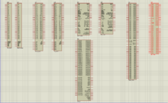
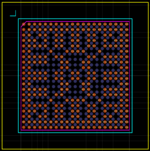
I've sketched out pin lists and packages to see how viable this is. However my patience today doesn't reach enough to finish bonding both parts together and then connecting the right pins to the right places on each device.
1688328649565.png
1688328730035.png
 

GRudolf94

Well-known member
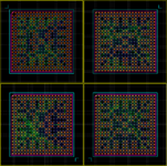
Here's all signals wired together between footprints. Ok, almost all signals, there's like 5 or 6 small details missing but the voltage rails, ground and 60x bus are all there. Honestly I don't think this is routeable in any of the 4 orientations shown here, within the space an interposer would need, within the constraints the CPU would need to operate, let alone at a reasonable cost for this to be worth for a hobby project that would then be difficult to assemble, even if there was no other risk to proper functioning. Before anyone asks, the CBGA360 PPC750 footprint has been mirrored properly.

1688354304382.png
 

cobalt60

Well-known member
It is looking to me like vias could fit in the middle of 4 pads, but I am new to this so not really sure. How many layers is this?

Since a large number of these could fit on a single panel, wouldn't that save a significant cost?

Anyway, it's fine if it's not economically viable, I still want to design this, and if it's too expensive to manufacture, then so be it.

The stock G3 ZIF modules are often found for around $10, and the 733MHz 750FX is currently available for $15. So even if the interposer did cost say $110, that's $135 in parts. So selling for $235 you'd make $100 for the labor. A little underwhelming for sure, and that's assuming nothing gets destroyed. But this is primarily not a money making adventure for me. I really just want to practice CAD, and if I can get myself and some community members some 733MHz G3 modules to be used as upgrades, it's just icing on the cake.
 

Bolle

Well-known member
What about just harvesting the PGA arrays from those 233MHz modules to reuse them and design a ZIF module that takes the 750FX right away.
 

Siliconinsider

Well-known member
A company did a 750L to 750GX interposer, it probably is not doable in less than 8 or even 10 layers considering how little room there is. My adapter is a clone of the powerlogix one, and it cannot be done with less than 8 layers. The thread is here: https://68kmla.org/bb/index.php?threads/ppc750gx-vs-ppc750gl.39043/

There are well known BGA escape routing, look for dog bone.

A cool alternative would be to pull the G3 out of ZIF CPUs and solder a 7400/7410 in place of the 750. This would at least help training in BGA reflow which is not an easy thing to do.
 

herd

Well-known member
Powerlogix did both the ZIF board and adapter board we're talking about. Has anyone asked OWC what it would take to open the Powerlogix archives?

Also, I think the 750FX has a 1mm grid pitch (vs 1.27mm).
 

GRudolf94

Well-known member
@cobalt60 you'd need via-in-pad, and blind/buried vias. 6 layers miiiight be doable on a stretch but I'm betting 8 really due to signal integrity. (you need vdd/ovdd/gnd ref planes)
 

GRudolf94

Well-known member
@Bolle I've been considering doing that (though reballing the PGA grids might be a bit annoying), or just making a separate PCB to act as a substrate, and then tacking mill-max (or similar) pins to the backside of that with solderpaste, and then that to a new PCB. Would also sort a few of my non-Mac uses.
 

cobalt60

Well-known member
I do plan to make or have made 7410 modules, but that seems really straight forward. I guess, can the pinout of the cache chips be counted on to match the ones pulled from the G4 modules?

Back to 750FX; if the cache chips are removed, then the interposer could be twice (or more) as big, extending into the area where the cache chips were. I think that would help with the limited space, though potentially cause issues with dealing with high frequency. Any advice on which traces should be shorter and which could be longer?

As far as the option of just designing a whole new ZIF module; is the pinout of the PGA available?
 

Phipli

Well-known member
I do plan to make or have made 7410 modules, but that seems really straight forward. I guess, can the pinout of the cache chips be counted on to match the ones pulled from the G4 modules?
The trap to watch for with this is that the 7410s dropped support for one of the voltages that older cpus supported if I remember right. I was looking at this and needed replacement cache chips, but the supplier let me down.
 

GRudolf94

Well-known member
@cobalt60 control signals aside, the 60x bus has 64 data lines (organized as DL31:0 and DH31:0), and 32 address lines (A31:0). You'd want all data lines to have minimal skew, ditto for address lines. There's also some control lines that have to be kept within the same group (offhand, !ARTRY, !BG, !BR and some others?). This is a much easier task on a 66MHz bus, there's plenty of room for sloppiness there. At 100MHz you get a bit less leeway.

Moving the focus of the subject a bit, honestly, my personal opinion is that if you want to get started on PCB design, a high speed, high density BGA design is the absolute wrong place to begin. It may seem annoying to have to tread thru the basics, but coming from someone who committed that exact same mistake, it's better to start from the start.
There's already plenty of room for error on simple stuff, as you'll probably learn. When I started doing this professionally, and crucified myself for a couple routing errors that could be bodged over, I got told "you should stop doing this - it's perfectly normal for boards to go in the trash because the mistakes in them make them completely unusable".
 

cobalt60

Well-known member
You do not need to replace the L2 cache. The 7400/7410 is a drop in replacement to the 750.
a stock 266MHz 750 module runs the cache at 133MHz, and a stock 533MHz 7410 module runs the cache at 266MHz; wouldn't I want those faster cache chips?

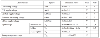
The ZIF module is a standard IBM/Motorola product that is documented here: https://datasheets.su/DS/NXP/MPCPCMEC.pdf
beautiful, thank you

This is a much easier task on a 66MHz bus, there's plenty of room for sloppiness there. At 100MHz you get a bit less leeway.
I'd actually personally be happy with 66 to 83MHz, but yes 100MHz would be ideal
 

herd

Well-known member
If you get anywhere with these, a Dual G3 would be a nice result. Dual G4 upgrades were made:


Phipli

Well-known member
If you get anywhere with these, a Dual G3 would be a nice result. Dual G4 upgrades were made:

Do you mean two G3 chips? I thought the G3 didn't include the hardware to support multi processors. Only the 601, 604, G4 and G5 did?

The beBoxes did it their own weird, unsupported way with the 603.
 
Top