hyperneogeo
Well-known member
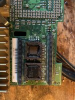
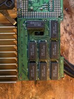
So I was looking at the L2 cache card and noticed that it had 32 pads for each chip, but was using only 28 of them for 32x8 (256k).
The original chip on there is: https://www.datasheetarchive.com/pd...516765643adf153033d176e&type=O&term=KM68257BJ x8
Looking at the pads, I see they are all connected (except pin 1 which is NC) and do match for example 128kx8 (1mb) :
Where as CE2 is suppose to be high (which is the original VCC for the 256k chip, so that's fine). All of the other pins are actually connected to each other and going to the connector.
Seeing how there is no 32 pin 256k chip afaik, maybe they were planning on upgrading the cache later own the road?
I actually tried replacing all of them with the 128kx8 chips an of course got the death gong. So my guess is the GAL at the bottom is controlling it some how? Luckily the gal itself was unlocked, so I dumped it. I have attached the gal. (Btw I'm aware the MC88915TFN133 isn't there, I just took it out)
Any thoughts?