• Hello MLAers! We've re-enabled auto-approval for accounts. If you are still waiting on account approval, please check this thread for more information.

Seeking Dove Marathon 030 Racer with cache for Plus/SE Accelerator Info (JED files, pics, or existing work!)

Oh crap, I totally forgot about that...
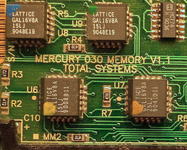
The GALs are available over here on the PLD archive and see the attachment for the schematics if the RAM board.
Thanks to the invaluable help of @JC8080 , the schematics for the Mercury 030 RAM board shared by @Bolle have finally been corrected. I've tested them with the RAM ICs (AS4C1M16E5) used in the standalone 4MB RAM board for the 128/512K, and it simply works!

Moreover, it works with the EDO version of these RAM chips. This is a big deal since I haven't been able to find authentic FPM versions (the ones I bought on Amazon turned out to be fake).

JC8080 bought a Mercury board with the RAM expansion a few years ago. Coincidentally, he bought it from the person who posted some nice pictures of it on Reddit. I actually contacted the original owner a few weeks ago, but he told me he had sold it. It turns out the buyer was JC8080!

If anyone would like to make an exact replica of the original RAM board for the Mercury 030 accelerator, or even integrate it into the Performer accelerator board, whether using the original 30-pin SIMMs (80ns or faster for 0 wait state) or these high-density RAM ICs, it can now be done!

The corrections are as follows:

Pin 4 of RU1A needs to be pulled up, so it should be connected to pin 1 or pin 10. If left floating, it corrupts the output pulse used by the synchronous part of the FSM for RAM refresh.

CLK for RU9 is CLK_30. (CLK_30 and SM_CLK16 are the same signal but are driven separately).

The "Big One": This had me scratching my head for months! Pin 12 of RU9 is actually DSACK1 for 32-bit data transfers, so it is connected to the other DSACK1 output generated on the accelerator board (pin 12 of U4). Checking the equations, it makes perfect sense: these two outputs are never driven by the PLDs at the same time. The DSACK1 from the RAM board only becomes active when the Fast RAM is being accessed; otherwise, it is tri-stated (the same thing happens with DSACK1 from the accelerator board for 16-bit onboard RAM accesses). DSACK0 is generated exactly like DSACK1 from the RAM board, which now seems pretty obvious since both DSACKs must be low for 32-bit word transfers.

That’s it for now!

It is important to add that the only driver that has worked for me (with or without the 32-bit RAM expansion) is the DOVE Racer 030. None of the "Gemstart" drivers out there seem to work in my prototypes. Interestingly, the "External Data Cache" functionality now seems to be activated when selected (the driver icon now shows the word CACHE); I don't know yet if it makes any difference.
 
Last edited:
What's the maximum amount of memory the Mercury 030 can address?
How would you integrate the RAM expansion logic into the Performer? At a glance, the Mercury 030 GAL U3 seems slightly different than the Performer's GAL U3.
 
What's the maximum amount of memory the Mercury 030 can address?
4MB. The way it works is by replacing the system RAM with 4MB of 32-bit RAM. It only 'switches' back to the system RAM for a small 32 KB region at the top where the video buffer resides. This logic can work on any early Mac that uses the stock Macintosh Plus ROMs.

Other Total Systems accelerator models can handle up to 16 MB of onboard RAM. Connectix Virtual is a must in order to access that extra RAM.


How would you integrate the RAM expansion logic into the Performer?

Just add the schematics shared by Bolle (with the corrections mentioned) to your Performer schematics. All signals are labeled accordingly to match the original schematics (PDF file) which you can find on his GitHub page.

It is up to you whether you want to implement the original RAM ICs (30-pin SIMMs) or the RAM ICs I tested.

Here are the schematics for the new RAM ICs:


RAM.png

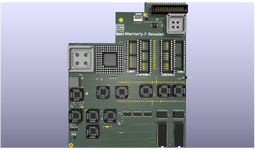
Let's say the hard part is the PCB layout for the Macintosh Plus and SE that integrates the new components. I made a custom PCB layout (currently in the prototype stage) for the Macintosh 512K that also integrates the SCSI I/O interface and the option of use stock or custom ROM ICs (ROM-INATOR)

Mercury_Reloaded.png

I would like to call it 'Mercury Reloaded.' It's more appropriate than 'Performer Fusion,' since the Mercury 030 board was intended for the Macintosh 128/512/Plus, while the MM Performer can't be installed on a Macintosh 128/512K.

The U7 chip is optional; the 16 MHz clock can be fed to it from the logic board, just the same way the Mercury board did.

At a glance, the Mercury 030 GAL U3 seems slightly different than the Performer's GAL U3.

Yes, you're right! There is a little difference in how it handles the NOFC signal. I used the GAL dumps from the Mercury board; I haven't tested the MicroMac Performer GALs yet.
 
Last edited:
I’m certainly not an expert in 68030 architecture (I’m sure others here could give a more precise technical breakdown) but this is a really interesting question. Honestly, I asked myself the exact same thing when I first started digging into this project.

In my opinion, the short answer is no: 0 wait-state DRAM doesn’t strictly negate the need for a cache. However, at 16 MHz, it makes the lack of a cache much less painful than it would be at higher clock speeds.

The RAM expansion logic on the Mercury 030 uses standard asynchronous bus cycles via DSACK signals (which usually take a minimum of 2 or 3 clock cycles) . A proper cache controller (or even a RAM expansion using the synchronous STERM signal) can take advantage of the 68030's Burst Mode. So, while this accelerator with the fast RAM upgrade is snappy (running 2-2-2-2 timing) a system with a cache could theoretically be faster on memory fills by using burst mode.

Exactly how much faster is hard to say, considering these early Macs have to switch back every 1/16th of a second or so to access the screen buffer in that slow system RAM. I really don't know how that specific overhead balances out in real-world use.

I’d say the next feasible step up would be using SRAM instead of DRAM in synchronous mode. From what I’ve gathered, you’d need SRAM ICs rated at 35ns or better to handle the tight timing of 16 MHz burst cycles. On the plus side, the logic would actually be simpler than the actual DRAM controller since you don't have to worry about memory refresh cycles, which might even mean needing fewer GALs.
 
Last edited:
SRAM at that speed is still much more expensive than DRAM even today. And you would need to write your own logic, which is not something I understand.
 
Besides the corrections already mentioned, there is another subtle issue:

One of the PLDs on the original RAM expansion board is 25 ns while the other three are 15 ns. Coincidentally, this PLD outputs the four CAS signals.

This may well explain why I am experiencing instability issues with my prototype; a stress test or minimal thermal drift induced on the RAM ICs immediately causes the system to crash. That 10 ns delay difference is almost certainly intentional and part of the original design.

Screenshot 2025-12-27 at 5.14.31 PM.pngRU7),
 
Back
Top