• Hello MLAers! We've re-enabled auto-approval for accounts. If you are still waiting on account approval, please check this thread for more information.

How did the PowerPC 603 / 5200 at 75mhz compare to PC:s (486/Pentium)?

Hi @Melkhior !

A really informative reply, thanks!
It seems I should clarify my "era" comments :) I didn't mean the whole 80s/90s<snip>
Aaah, OK.
Of course the RISC designers were very much aware of the memory issue - "underestimated", not "ignored" :) The trick was that, like their 68k-based predecessors, early RISC workstations (not personal computer!) had large caches<snip>
Good point. Applying Personal Computer cache compromises to RISC, cut the performance down to PC speeds.
<snip> the RISC vendor <snip> to an extant thought their performance lead was due to the "better" design of RISC vs. CISC <snip>.The new batch of RISC CPUs I listed above were great (with the SuperSPARC being the best of course, as I'm a SPARC man), but when the P5 <snip>, the lead was much smaller <sinp> economy of scale <snip> enough internal cache <snip> 64-bits bus to feed the CPU, same as most others, and that was enough to close most of the gap <snip>
Yes.
How the code is built <snip> irrelevant, unless <snip> poor support for calls to dynamically loaded functions. The issue was <snip> from a bunch of loops that had made the bread-and-butter of CDC & Cray in simulation codes, to <snip> interactive use with graphics (the 3M <snip> recompiling a bunch of codes<snip>.
Sorry about butchering that para. Again, good points. CF: SGI O2 UMA architecture, precisely because locality rules changed with multimedia GUIs. Arguably, this has now come full-circle, because Apple's M series of computers (I'm underutilising my MacBook M2 to write this) employs tight NUMA style architectures, but this time coupled to multiple cores. Arguably though, again, it's the tight coupling of high memory bandwidth to multiple, but simpler CPUs that now provides better system performance/Watt.
<snip> pipeline in RISC!" works if you have enough ILP to extract, and ILP from indepedent iterations of loop is almost unbounded <snip> between you loads. Indirect accesses don't play very nice with memory hierarchy, either...
Yeah. It was easier to pipeline scalar and early superscalar RISC CPUs. However, even in "Computer Architecture: A Quantitive Approach 2nd Edition", the limits of ILP were already being reached. The R4000's super-pipelining as an early attempt; then increasingly complex scoreboarding, reservation stations and register renaming + more pipeline stages to extract ILP became very apparent.

It could be argued though that the Pentium 4 was the first real casualty of the ILP wars; as CPUs started to shift to multi-core designs. This was the point where Intel started to falter.

It was also important in the workstation/server markets in the 90s <snip> CPU2017 being the current one <snip> "rate" and not "speed", as single-process benchmarks on 64+ cores CPU don't make much sense.
Yes. Grunt matters most in that market.
<snip> Does having more registers give you performance... or do you *need* more registers because otherwise you don't get any performance? The P5 and P6 (vs. all the RISC of the era) eventually proved IMHO that there's no absolute answer, and that various trade-offs are viable. In ASIC design, logic is cheap, memory is very expensive, and registers are memory.
I sort-of agree, but I think I'll try and offer my opinion on that at the end of this comment.
The original ARM1 has a *lot* of area dedicated to the register file. It's a choice, and clearly they were doing something right as Arm is still around.
Herman Hauser: "I gave our engineers two things Motorola and Intel never gave their teams. Firstly, I gave them no people and secondly, I gave them no resources. The only way they could do it was to make it as simple as possible."

What did Acorn get right? Two things, really. Acorn were facing the same issue as all other home computer manufacturers after the 8-bit era. Do they just start building, boring, bland, x86 PCs or do they try and differentiate? Sinclair, Atari, Apple and Commodore all picked different 68K solutions. Sinclair's QL went for a cheap, preemptive, multitasking business computer (I had one in my undergrad days & loved it). The QL failed because the 68008 was underpowered and the ROM was too buggy. Atari got lots of money from Tramiel to build the equivalent of a 16-bit ZX Spectrum: Fast & colourful enough for the masses, but without enough investment and industry support it died. The Amiga survived for a while thanks to its amazing chipset (but Commodore failed to then update it fast enough). Apple went for an underpowered, but easy to use GUI computer and survived (astoundingly), because they did keep updating it.

Acorn had none of these things. IMHO ARM survived because it was so minimalist it ended up being the CPU of choice for the Newton and then the CPU of choice for advanced embedded systems, thanks to the licensing model Apple forced on ARM, the company. I think this is Steve Furber's viewpoint.

<snip> remain a RISC fan,
Yay! I think you can tell I'm a RISC fan given my devotion to defending the 603(e) :D... :rolleyes: !
<snip> guidelines than actual rules, and they should be ignored if it helps with performance and/or versatility of the software<snip>
Which I think is how Hennessy & Patterson define it.
I'm not sure the data supports that conclusion for integer. in SPECint89, the 486 is better than the low-end SPARC, 33 MHz PA-RISC, and cacheless RS/6000 <snip> non-existent CPUs, which anyone can do<snip>saved me a ton of grief waiting on empty promises.
I noticed that. I assumed the 33 MHz Low-end Sparc came out when the 486 was still running at 25MHz, so I glossed over it and foolishly hoped you wouldn't realise ;) .
As for FP, yes the 486 <snip>, back then if you didn't <snip> a lof of systems with no FPU, and that was perfectly fine <snip> Why pay through the nose for a feature you don't need?

Ultimately, people buy hardware to run software. So the criteria really are (a) can it run my software ? (b) can I afford it ? And the ultimate choice is usually the cheapest system that is "good enough" for the software... UNIX workstations were expensive by a lot larger margin than they were faster in the 90s, while the 486, P5 and cheap PPC systems were "good enough" for a larger and larger fraction of the existing software. (I still love my Sun Ultra 1 Creator 200MHz which I bought brand new :) ).
Bringing it back round. I highlighted "economy of scale", "more registers because otherwise you don't get any performance", "various trade-offs are viable", "registers are memory". One way of looking at RISC is that it's an optimisation strategy that helps the little fish compete with the big fish. And the ultimate point of that is that if they can't compete, it's not an optimisation.

So, RISC-I, MIPS and RISC-II were a way for student CPU designs to compete with the DEC VAX. ARM was a way for Acorn to keep selling proprietary computers to the British educational market in the face of the dominant PC market (which was already selling into UK education). Sparc, later MIPS, et al were a way for Sun and SGI etc to carve out a high-performance market. The IBM 801 was a way for IBM to compete in the telephone switching market, but then the RS/6000 was a way for IBM (a little workstation fish) to compete with big workstation fish. PowerPC was a way for Apple to compete against the Wintel duopoly (arguably, given the effect of PPC clones on Apple, x86 Macs in the 90s would have been even more devastating, Apple would have gone the way of NeXT).

And to finish. People don't always just buy hardware to run software, sometimes they buy it out of spite :) . I bought this :) MacBook M2, because the company I was working for offered(threatened) to provide me with an extra Windows Laptop if I dared to use my own Intel MacBook Pro to VPN into my work laptop again (it had snowed overnight so I and quite a number of other employees had VPN'd into work on their home PCs.. but only the Mac was frowned upon for doing that).

Now I'm back in the little-fish world of RISC and it feels sooo refreshing! Have a great day!
 
Hey Julz!
Really? From my reading of the manual:

The Instruction cache bus is 64-bits wide, so it has to read one 64-bit word per cycle in order to feed two instructions to the IQ per cycle. Or do you mean the data cache?

Credible. Is this for the critical word or for the entire 8 word burst?
Oh yes, I was referring to data cache, I thought you were as well 🙃


TLB misses have to be handled in software. I'm sure you have a good source for this
The best source. My empirical benchmark of the L2 cache on a 5200 :D

, but such a cost for a TLB miss would be basically insufferable. From this MPR article, the 603 has a 64-entry x 4kB TLBs giving 256kB of TLB hits, which.. Going by this recent post of mine:


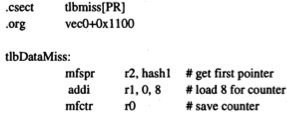
The miss rate is 0.9% for a 256kB cache, which might be similar for 256kB of TLBs. So, every 0.9% of instructions (and/or data), we'd have a 168 cycle hit. That's an average of a 1.5 cycle cost per instruction, making the 5200 terribly slow. However, the MPR report:

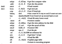
View attachment 76787
claims the TLB miss-handler can fit in two cache lines (16 instructions). The question then is whether the miss-handler itself is likely to be in L1, L2 or main memory. A miss-rate of 0.9% in any of the caches, will mean that most of the time, the TLB miss-handler will be in L1, bringing the handler code itself down to about 8 to 16 cycles; or an additional 4 cycles (12-20). Reloading a TLB will require, probably loading 64-bits from outside of the TLB, but some of these accesses themselves will be in the cache for the same reasons (TLB misses will also exhibit locality and a 0.9% miss rate means that most of the L1 cache and virtually all the L2 cache is likely to contain TLB data).

In the worst case though we'd need to load 16-words from main RAM for the handler = 32*16=512c, then probably 4 to 8 words from main RAM for the TLB data at 32 cycles per word = 128c to 256c => 640c to 768c. I think this is as bad as it'll get on System 7, because AFAIK, page tables can never be paged out to disk.

In either case, because the Pentium has hardware TLB miss table search it'll be much faster anyway.
It is a 168 cycle hit only on the first attempt to read a page that miss TLB, all subsequent accesses to that page that is not in L2/L1 is 32 cycles. So e.g. 320x240 framebuffer with 2 bytes, that is 38 pages, going through it all, the TLB overhead is 168 * 38, so it is not too bad unless your access patterns are random across > 64 pages, which you essentially by design should avoid. Avoiding that may cause you extra compute though (e.g. triangles sorted in z, can be arbitrary where they end up in the framebuffer, so may activate 38 pages, and same with a 256x256 texture (16 pages), now you have only 10 other pages. You can clip your framebuffer in half, so that you render e.g. top and then bottom, reducing risk that you swap around TLB entries (I have not done that, but should try to see if that helps).

Indeed, and is it the case that the 5200 can't use FPM mode? Is it really that bad? A 75MHz 603 needing 32 cycles for a main RAM read implies 32/75=426ns RAM access times from, I believe 70ns RAM?

Doesn't this part of the Pentium manual contradict what you're saying?
View attachment 76788
The Pentium's FPU is integrated with the Integer Unit on the U pipeline:
View attachment 76790
View attachment 76791
Because the FPU is integrated into the U pipeline (apart from FXCH); no instruction can enter either pipeline until both pipelines complete their WB stages; and the FPU bus is shared with the U pipeline for most operations, I think this means that the FDIV will stall integer operations in both pipelines.
Empirically, for sure it does not stall both pipelines or else Quake 1 would not have worked at all :D. Michal Abrash's perspective texture mapper did the division using fdiv for every 8 pixels, and while those pixels were being texture mapped using the integer units the next fdiv was calculated. It could be that the majority of those 33 cycles the fdiv took, it is not stalling the u pipeline and is being executed only in the FPU? Would you perhaps have the pentium manual handy to be shared?

I had some more comments but time's up for this time :D

btw my code environment: mostly Linux gcc, Mac clang, and then I do the final build on CW Pro 7.1 (on my PBG3) or CW Pro 5 (on my 5200), when I do experiments for performance it is more on the 5200.

Cheers
 
Hi @noglin,

Nice shooting!
Oh yes, I was referring to data cache, I thought you were as well 🙃
I was thinking about Instruction access as a limitation on performance. However, I would have assumed the Data Cache performance was the same as the Instruction Cache.
The best source. My empirical benchmark of the L2 cache on a 5200 :D
I've read the post now - scary. I've tried to understand it, but my wife & friend have alternate episodes of "Only Connect" and "University Challenge" on iPlayer, so I'm somewhat distracted ;-) !
It is a 168 cycle hit only on the first attempt to read a page that miss TLB, all subsequent accesses to that page that is not in L2/L1 is 32 cycles. So e.g. 320x240 framebuffer with 2 bytes, that is 38 pages, going through it all, the TLB overhead is 168 * 38
OK. For a start, it makes your demo all the more impressive! I'll try and break the 32 cycle reload down a bit more and ask why. Clearly, if the access time was 32 cycles, then that means we'd be dealing with 32/75*1000=426.67ns cycle time RAM, when in fact we know. Video DRAM is 60ns; DRAM must be 80ns or less (p47). "The RAM controller in the F108 IC supports line burst transfers." OK, so we also know it does FPM mode.


I had a look at this data sheet:

On the 60ns chips, full reads, I think take 60ns, FPM reads take 35ns. So, guessing, for 80ns DRAM; full reads take 80ns, FPM reads might take 45ns. If we assume for the moment that the L2 cache line length is the same as the L1 cache line size (32 bytes) and that the full line must be read into the L2 cache before any word can be read from the L2 cache to the CPU and that a full line can be read as one full access + the rest as FPM. What's the timing? 32 bytes=8 x 32-bit words. That's 45ns*7+80=395ns. Then we have another 32ns left, which is 1000ns / (1/1MHz) = 2.4 cycles. So, it's possible with an early word first transfer, we get the first word then.

OK, so I think we have an explanation for that. The figures might be a bit out, but they make sense. I won't yet speculate why a TLB miss takes 168 cycles when supposedly a simple miss routine takes two cache lines, which would still likely be in the instruction L1 cache.
Empirically, for sure it does not stall both pipelines or else Quake 1 would not have worked at all :D. Michal Abrash's perspective texture mapper did the division using fdiv for every 8 pixels, and while those pixels were being texture mapped using the integer units the next fdiv was calculated. It could be that the majority of those 33 cycles the fdiv took, it is not stalling the u pipeline and is being executed only in the FPU? Would you perhaps have the pentium manual handy to be shared?
Pentium manual from here:

Post supporting your claim about Quake:
 
I've read the post now - scary. I've tried to understand it, but my wife & friend have alternate episodes of "Only Connect" and "University Challenge" on iPlayer, so I'm somewhat distracted ;-) !
Is it the 32 cycles you find scary? Or the post? :D

OK. For a start, it makes your demo all the more impressive! I'll try and break the 32 cycle reload down a bit more and ask why. Clearly, if the access time was 32 cycles, then that means we'd be dealing with 32/75*1000=426.67ns cycle time RAM, when in fact we know. Video DRAM is 60ns; DRAM must be 80ns or less (p47). "The RAM controller in the F108 IC supports line burst transfers." OK, so we also know it does FPM mode.


I had a look at this data sheet:

On the 60ns chips, full reads, I think take 60ns, FPM reads take 35ns. So, guessing, for 80ns DRAM; full reads take 80ns, FPM reads might take 45ns. If we assume for the moment that the L2 cache line length is the same as the L1 cache line size (32 bytes) and that the full line must be read into the L2 cache before any word can be read from the L2 cache to the CPU and that a full line can be read as one full access + the rest as FPM. What's the timing? 32 bytes=8 x 32-bit words. That's 45ns*7+80=395ns. Then we have another 32ns left, which is 1000ns / (1/1MHz) = 2.4 cycles. So, it's possible with an early word first transfer, we get the first word then.
Nice, although I'm not convinced (yet). While the numbers match the empirical values, it is assuming that the RAM is the bottleneck and that a full line must be read into L2, while the bus and cpu has a "critical word first". Also, if RAM was the bottleneck, then VRAM read would be about the same, but it is about twice as slow (50-70 cycles, as I recall). Could it instead be the bus itself? It is at 37.5 MHz and probably requires several cycles to communicate the address and then pass the data and the ack?

(I am also eager to hear thoughts on why the vram read is slower than the ram read, I wish there was some magic way to read vram faster....)

OK, so I think we have an explanation for that. The figures might be a bit out, but they make sense. I won't yet speculate why a TLB miss takes 168 cycles when supposedly a simple miss routine takes two cache lines, which would still likely be in the instruction L1 cache.
Even if it was only 8 instructions (2 cache lines) it would be a loop that would walk through the page entries until the right one was found. Why I saw consistently 168 cycles I'm not sure of actually, one could imagine that it would be more varied if the search itself was the bottleneck.

Btw, these 168 cycles is not too much of a problem. The example before: 320x240x2 = 38 pages, access that linearly is an overhead of 38*168 cycles worst case, which is negligible compared to cycles available per frame (75/30fps = 2.5M cycles per frame). Having multiple large textures though requires some more care.
OK, I think I found the explanation, the fdiv likely only blocks the u unit for a few cycles, and spends majority of time in "floating point execute stage two". I suppose any subsequent instruction that had a dependency on the fpu result would at that point stall.

3.6.1
The Pentium processor FPU has 8 pipeline stages, the first five of which it shares with the
integer unit.
Integer instructions pass through only the first 5 stages. Integer instructions use
the fifth (Xl) stage as a WB (write-back) stage. The 8 FP pipeline stages, and the activities that
are performed in them are summarized below:
PF Prefetch;
D I Instruction Decode;
D2 Address generation;
EX Memory and register read; conversion of FP data to external memory format and
memory write;
Xl Floating Point Execute stage one; conversion of external memory format to internal FP
data format and write operand to FP register file; bypassl (bypassl described in the
"Bypasses" section).
X2 Floating Point Execute stage two;
WF Perform rounding and write floating-point result to register file; bypass 2 (bypass2
described in the "Bypasses" section). .
ER Error Reporting!Update Status Word
 
Thanks for sharing your results. Would you consider uploading your build? There are not many entries with results from these computers for comparison. Does CW7.1 also build for 68k? This thread might be a good place for it:
Sure, I'm not near the machine where I have it now, but will do once I am.
 
The Amiga survived for a while thanks to its amazing chipset (but Commodore failed to then update it fast enough). Apple went for an underpowered, but easy to use GUI computer and survived (astoundingly), because they did keep updating it.
My long-standing position is the Amiga died *because* of its "amazing" chipset, while Apple survived because of the lack thereof and the willingness to break some stuff during the Plus => II transition.

With the "amazing" chipset (Amiga and others of the era), software is tied too closely to the hardware. Backward compatibility with software was to be the key factor for the PC (and to a lesser extent Mac) success, which wasn't obvious yet though there were signs. For instance, the original vision that was driving the RISC/UNIX crowd was that the hardware was to be optimized at each new silicon generation, and the software would be C on UNIX and therefore portable from one generation to the next simply by recompiling... and that's not exactly what happened. It remains in the name of the "Microprocessor without Interlocked Pipeline Stages", which added interlocked pipeline stages in the second iteration because they needed to be software-compatible and hardware constraints had changed...

New Amigas (ans STs, ...) needed to support old software (read: games) with highly timing-dependent optimizations, while Apple broke the 512x342 B&W games with the II and never looked back. That decision might have crippled gaming on Macs at one point, but the key markets didn't include gamer for the Mac back then.

Which I think is how Hennessy & Patterson define it.
Tell that to the RISC-V decision-makers... my examples were not random :->

I noticed that. I assumed the 33 MHz Low-end Sparc came out when the 486 was still running at 25MHz, so I glossed over it and foolishly hoped you wouldn't realise ;) .
The 33/40 MHz variant of SPARC were a late update, at that time the microSPARC and SuperSPARC were the future (both appeared in '92). SPARC (the original one, with multiple hardware implementations) was V7 and the lack of integer multiply had become an obvious issue; once introduced, everyone wanted V8 hardware for anything but the low end.The SLC/ELC (17" B&W monitor with a small motherboard at the back) were always entry-level systems. For fairness to SPARC, a SPARCstation 2 or an IPX (both with a 40 MHz SPARC) would have been better choices, but they were also much more expensive than ELCs.

It's also quite difficult to compare apples with apples so long after the fact; things were moving very fast, and the 'best' system could change on a quarterly basis with so many players. There was only 18 months for the SS2 to be the highest-end pizza box from Sun before the 10 was introduced. The IPX had 16 months shining before the SPARCclassic (with a V8 microSPARC). It would only be another 16 months or so before the SS5 showed up (microSPARC II with much higher clock than the original). 20 months after the SS5, the Ultra 1 was introduced with the new 64-bits V9 architecture (and more usable atomic operations, which was quickly becoming an issue for the performance of SMP SPARC where Sun had followed Solbourne). V8 only had from May '92 [1] to November '95 as the high-end SPARC architecture at Sun. Yet it was important enough to become IEEE Standard 1754-1994, and kept selling for a while after that (clones using Ross HyperSPARC mostly).

Bringing it back round. I highlighted "economy of scale", "more registers because otherwise you don't get any performance", "various trade-offs are viable", "registers are memory". One way of looking at RISC is that it's an optimisation strategy that helps the little fish compete with the big fish. And the ultimate point of that is that if they can't compete, it's not an optimisation.
Also an important driver of simplicity is time-to-market. If it's easier to design and verify, it's faster to market and more competitive.

And to finish. People don't always just buy hardware to run software, sometimes they buy it out of spite :) .
But we're in the minority in terms of volume and revenu :-) (I bought my AluBook in '05 knowing full well PPC was dead and x86 the future at Apple, but I wanted to resist as long as possible...).

[1] Actually, the 600MP shipped before the SS10 (late '91), but I'm not sure when the SuperSPARC option became available, as it was also sold with one or two dual-SPARC (regular V7 SPARC) module called SM100. I have some of those, and you can actually run NetBSD in a SPARCstation 20 with four regular V7 SPARC (instead of SuperSPARC or HyperSPARC) You really don't want to, but you can :-). V8 might have had 4 full years at the high-end.
 
Hi Noglin,
Is it the 32 cycles you find scary? Or the post? :D
Despite my frequent errors, I'm enjoying this thread. I've been getting more despairing about the PPC 603(e)'s performance vs Pentium as I read your replies, but then when I read the Bitsaver's manual, I start to regain some admiration for it ;) ! But maybe you don't feel terrible about the PM5200 and the 603, it's that you feel it's a fun challenge to exploit its capabilities vs its weaknesses! 'Scary' refers to the post, or rather the figures in the post, which I guess partly includes the 32 cycles.
Nice, although I'm not convinced (yet). While the numbers match the empirical values, it is assuming that the RAM is the bottleneck and that a full line must be read into L2, while the bus and cpu has a "critical word first".
Well we know that there's a 64-bit bus to the L2 cache; that although it doesn't run on the '040 bus (where normal RAM is). That bus runs at 75MHz:

1723278690884.png
We know from the 603(e) manual that the 603<->L2 cache will load an entire L1 line at a time (32 bytes or 8 words) and that it will load the critical word first. So, that bit is correct. We know that the RAM controller supports burst transfers.

1723278976585.png

So, here's why I think my timing estimate is roughly correct. There's only one bus going from Valkyrie to the L2 cache, the 32-bit bus latched onto a 64-bit bus. It's the L2 cache that's going to make the cache line refill request from DRAM, because the CPU doesn't know about both caches, it just thinks it's talking to memory (just like on a PB1400/117 which talks only to SDRAM); that is, the CPU requests the specific address first, i.e. the critical word first, but the L2 cache doesn't have it, so it stalls the CPU, but the CPU doesn't make an additional request to DRAM, it must be the L2 cache that does that. The L2 cache won't request the critical word first, it will just fill its cache line, and the only way to make use of burst mode is to read the first word in the cache and then the other 7. Now I suppose that the 603, seeing addresses and data on the bus could load in the critical word when it sees it, but I don't think it does, because what it wants is the critical word, then possibly earlier words and only the L2 cache will do that.

Also, I've just noticed something interesting.. the transparent latch on the ROM / Cache card says: "P_A21-5", so bits 4..0 aren't there.. i.e. it can only reference addresses on a 32-byte boundary.
Also, if RAM was the bottleneck, then VRAM read would be about the same, but it is about twice as slow (50-70 cycles, as I recall). Could it instead be the bus itself? It is at 37.5 MHz and probably requires several cycles to communicate the address and then pass the data and the ack?
(I am also eager to hear thoughts on why the vram read is slower than the ram read, I wish there was some magic way to read vram faster....)
I think that's a fairly simple answer. The VRAM is really single-ported DRAM, so it's having to service requests for video generation as a priority and from the CPU. It's certainly going to be much slower and do we know if it handles burst mode? I think this can be calculated by guessing the number of memory requests needed to support 640x480x8-bit (for the transparent frame buffer used as a proxy for the actual scaled 320x240x16-bit frame buffer). It might be OK. I suspect it'll make 2 access per word of video, by reading 4-pixels from 640x480x8-bit then reading 32-bits from the 320x240x16 buffer (which is 2 pixels, but stretched); then on the next scan it reads from the odd line in the 640x480x8-bit, but the same 32-bits from the 320x240x16 buffer as it wouldn't have cached the 320x240x16 scan the previous time. So, that's 640x480/4 = 76800 x 2 = 153600 * 60 = 9.2 million fetches per second, which needs a read speed of about 109ns. So, I think, yes, it's already taking up over half the bandwidth of the video DRAM (unless it's also using FPM mode, in which case it's still a fair amount, about 25%).

Is there a faster way to read VRAM? Can't think of any yet.
Even if it was only 8 instructions (2 cache lines) it would be a loop that would walk through the page entries until the right one was found. Why I saw consistently 168 cycles I'm not sure of actually, one could imagine that it would be more varied if the search itself was the bottleneck.
The 603 TLB algorithm uses a primary hash, but also up to 8 loops:

1723280972566.png
1723281009229.png
At a minimum, it's going to be 21 instructions, approx 21 cycles (maybe a bit more) + 3 cycles per search => +21, so up to 42 cycles; average 33-ish. Then, if we need the second hash, it's another 7+up to 7 loops, so up to 70 cycles. If it fails that, I think it goes into a slower loop. I think that it's unlikely that it'll take all of them every time.

Btw, these 168 cycles is not too much of a problem. The example before: 320x240x2 = 38 pages, access that linearly is an overhead of 38*168 cycles worst case, which is negligible compared to cycles available per frame (75/30fps = 2.5M cycles per frame). Having multiple large textures though requires some more care.
OK.
OK, I think I found the explanation, the fdiv likely only blocks the u unit for a few cycles, and spends majority of time in "floating point execute stage two". I suppose any subsequent instruction that had a dependency on the fpu result would at that point stall.
3.6.1
The Pentium processor FPU has 8 pipeline stages <snip>
Agreed, I had misread the manual.. but it would have helped if the manual had said: "new integer instructions can resume once a floating point instruction enters the dedicated FPU pipeline.

-cheers from Julz
 
My long-standing position is the Amiga died *because* of its "amazing" chipset, while Apple survived because of the lack thereof and the willingness to break some stuff during the Plus => II transition.
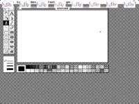
It's a good proposition. I might put a slightly different perspective on it. Apple made a big thing of programming to the Toolbox rather than accessing the hardware. We know that programmers did break the rules a bit: they/we made use of low-memory system variables and the A5 world. But as a whole, people stuck closely enough to make the Mac II a fairly seamless progression. Having said that (and I think you can simulate this on infinite Mac's Mac II), when you run MacPaint 1.5 in 8-bit colour:
1723305622905.png
Commodore never enforced an abstraction on using the CoPro or the rest of the advanced video hardware. So, I guess that did make it hard for them to change the hardware. PCs didn't start to enforce any abstraction until Windows 3.x and programmers wrote directly to the hardware all the time and games or other applications had to specifically target multiple, different video cards. This is what helped PCs become entrenched, because so much software was more difficult to port, but when PC graphics hardware caught up; the abstractions were now the convention and so it wasn't a problem. Unix systems, as you say, stuck to a high-level abstraction.
<snip> RISC/UNIX <snip> optimized at each new silicon generation, and the software would be C on UNIX and therefore portable <snip> by recompiling <snip> "Microprocessor without Interlocked Pipeline Stages", which added interlocked pipeline stages in the second iteration because they needed to be software-compatible and hardware constraints had changed...
Delayed branches also suffered the same fate. A performance advantage for single-issue architectures, but added complexity for superscalar CPUs.
Tell that to the RISC-V decision-makers... my examples were not random :->
Oh, yeah I read something about RISC-V designers making the same mistakes as everyone else.
The 33/40 MHz <snip.. Summary: 33/40 MHz V7 SPARC (late). microSPARC/SuperSparc ('92)=future. V8 Introduced MUL, so V7 relegated to low-end. AIO SLC/ELC=entry level, but SS2/IPX were better, but pricier.>
<snip> IEEE Standard 1754-1994, and kept selling for a while after that (clones using Ross HyperSPARC mostly).
I forgot early Sparc only had multiply step and divide step: Square root step can also be done with a slight mod on divide Step! It was a good idea to be able to licence Sparc. To me, your history description looks a lot like Apple's anarchic period in the mid-90s: too many architectural variations to support their market; whereas, until the late 386-era, Intel just had an upward-compatible succession of CPUs, despite much larger markets... well, they generally had 2 versions per generation: 8086/8088, 80186/88, 80286, '386/'sx/sl, '486/sx..
Also an important driver of simplicity is time-to-market. If it's easier to design and verify, it's faster to market and more competitive.
RISC developers did have that advantage, at least in the early days.
But we're in the minority in terms of volume and revenu :) (I bought my AluBook in '05 knowing full well PPC was dead and x86 the future at Apple, but I wanted to resist as long as possible...).
Ditto: I bought my PB G4 12" in late '05, just before Apple went Intel, so that I could avoid going Intel for a few years (I eventually bought my first Intel Mac, a 2006-era MacBook Core Duo in 2010).
[1] Actually, the 600MP<snip>
Also, interesting.

-cheers from Julz
 
My long-standing position is the Amiga died *because* of its "amazing" chipset, while Apple survived because of the lack thereof and the willingness to break some stuff during the Plus => II transition.

I take the same position. The chipset was a fatal straitjacket for expanding the hardware, and both it and AmigaDOS were sufficiently limited that software had to (ab)use it in weird ways that made backwards compatibility impossible. The chipset was all but deliberately designed to make scrolling-background games hard to program, while almost all other hardware of the time (including the Commodore 64) was designed around that being the natural way to do things.
 
I take the same position. The chipset was a fatal straitjacket for expanding the hardware, and both it and AmigaDOS were sufficiently limited that software had to (ab)use it in weird ways that made backwards compatibility impossible. The chipset was all but deliberately designed to make scrolling-background games hard to program, while almost all other hardware of the time (including the Commodore 64) was designed around that being the natural way to do things.
I wanted to check this out a bit and found this blog, by the guy who wrote Uridium 2 for the Amiga (an upgrade from Uridium):


Are the methods for writing this scrollling game (which scrolls in 2 dimensions) really much harder than for a C64? I don't know much about the Copper, the blitter or the sprite engine; I once had a friend who used to wax-lyrical about the abilities of the Amiga so I'm prone to glorifying it somewhat, but the descriptions of how the scrolling worked are pretty similar to how I imagined it would work: an extra 16 pixel wide character's width on the bottom and right which is gradually exposed by changing the x offset and then the video start address is moved on 2-bytes when we've scrolled 16-bits.

Here's a conversation about background scrolling:


At one point, a poster favourably compares the Amiga implementation of James Pond with the Jerky Archimedes version.

I'd still like to return to the idea that the chipset wasn't the problem. Here's some more of my reasoning:
  1. In the PC world, these things made no difference. It didn't matter if there was multiple graphics architectures: CGA/EGA/VGA(MGCA)/Hercules/SVGA and then later chipsets with increasing hardware support.
  2. In the PC world it didn't matter if they had to write directly to the hardware or use OS APIs or DirectX, it was still a success.
  3. In the Video console world it didn't much matter if they switched CPUs or had totally different graphics architectures: most consoles did really well (with the exception of the N64 or Sega Saturn and although Sega didn't seem to survive the Saturn failure, Nintendo did prosper after the N64).
  4. In the Mac world it didn't matter that the compact Macs had 1bpp x 512 x342, with no hardware assist, then the Mac II had indexed 8-bit graphics and subsequent Macs had increasing or varying hardware assist (which is part of the conversation about Valkyrie's pixel-doubling mode).
  5. In the Acorn world it didn't matter that the Archimedes had almost no hardware acceleration and the platform had a tiny market share mostly confined to the UK, they still managed to keep the platform going longer than Commodore did.
  6. Even for games that exploited the Amiga hardware, many games were converted between the ST and Amiga, so developers would have abstracted much of the lower-level graphics functionality. In a sense this is also what happens for Doom, running on different platforms: the game itself was developed on a NeXT computer and then ported to a PC before being ported to other platforms.
What all of these platforms and the companies behind them had in common was that they cared about the platform and improved the hardware over time. I figure if the Amiga had had worse graphics, it would have either gone the route of the Atari ST and died at a similar time, though arguably, the Amiga survived better thanks to third-party PPC boards and MorphOS. As I see it, the problem was really Commodore's lack of leadership. Despite considerable effort from engineers, they were more interested in milking the existing hardware than have a vision for the platform. They floundered trying to switch to PC computers, undermining confidence in the Amiga itself, much as Palm and Nokia did when it decided to switch to WinCE (or Windows Mobile as it probably had become).

Over to you!

-cheers from Julz
PS. I switched to using my early 2008 C2 MacBook, with a whole 2GB of RAM for this reply! Typing is slightly slower than on the other Macs, but still very usable! Geekbench 5: 321(SC)/580(MC), about 2x slower than my Mac mini 2012.
 
Hi Noglin,

Despite my frequent errors, I'm enjoying this thread. I've been getting more despairing about the PPC 603(e)'s performance vs Pentium as I read your replies, but then when I read the Bitsaver's manual, I start to regain some admiration for it ;) ! But maybe you don't feel terrible about the PM5200 and the 603, it's that you feel it's a fun challenge to exploit its capabilities vs its weaknesses! 'Scary' refers to the post, or rather the figures in the post, which I guess partly includes the 32 cycles.
Especially exploit its capabilities :D and an understanding of what *should* be possible gives me an idea of how to best do that, or what to avoid that is slow.

Well we know that there's a 64-bit bus to the L2 cache; that although it doesn't run on the '040 bus (where normal RAM is). That bus runs at 75MHz:
Actually, the 603 bus on the 5200 is running at 37.5 MHz (a multiplier of 2). One way to prove this is to measure the div instruction (37 cpu cycles) using the "tb" register. "tb" ticks once every 4 bus cycles, and I get exactly 37 cpu cycles with a multiplier of 2. I see 37.5 MHz also reported here and there as the system bus frequency for the 5200.

View attachment 76819
We know from the 603(e) manual that the 603<->L2 cache will load an entire L1 line at a time (32 bytes or 8 words) and that it will load the critical word first. So, that bit is correct. We know that the RAM controller supports burst transfers.

View attachment 76820

So, here's why I think my timing estimate is roughly correct. There's only one bus going from Valkyrie to the L2 cache, the 32-bit bus latched onto a 64-bit bus. It's the L2 cache that's going to make the cache line refill request from DRAM, because the CPU doesn't know about both caches, it just thinks it's talking to memory (just like on a PB1400/117 which talks only to SDRAM); that is, the CPU requests the specific address first, i.e. the critical word first, but the L2 cache doesn't have it, so it stalls the CPU, but the CPU doesn't make an additional request to DRAM, it must be the L2 cache that does that. The L2 cache won't request the critical word first, it will just fill its cache line, and the only way to make use of burst mode is to read the first word in the cache and then the other 7. Now I suppose that the 603, seeing addresses and data on the bus could load in the critical word when it sees it, but I don't think it does, because what it wants is the critical word, then possibly earlier words and only the L2 cache will do that.
This test was for RAM, i.e. 32 cpu cycles (16 data bus cycles) was for loading 4 bytes from RAM (so valkyrie would not be relevant here).
It seems odd that the critical word would not be used also for RAM? In the 603(e) manual, it does say that the cache will fill its line by wrapping around and that the first beat on the data bus is for the critical word. And the "543 D latches" seems to be a way for the CPU to get that critical word without waiting for the L2 to get the block?

8.3.2.3:
"... burst reads are performed critical-double-word-first, a burst-read transfer may
not start with the first double word of the cache line, and the cache line fill may wrap around
the end of the cache line."

Given the request from CPU to load 4 bytes, and we end up reading 32 bytes (due to the address being cacheable), given that we are now on 32 bit, it will be 8 beats.

I am not sure how this corresponds to transactions on the address and data buss, and any stall on the controllers etc, but just the transfer itself on the data bus would have to be at best 8 data bus cycles: 8/3.75*1000 = 213ns, that would be about 16 cpu cycles.

Also, I've just noticed something interesting.. the transparent latch on the ROM / Cache card says: "P_A21-5", so bits 4..0 aren't there.. i.e. it can only reference addresses on a 32-byte boundary.
OK I suppose that makes sense, because to go out on the 32 bit bus, it is either to write or read but only a full block. And I suppose the data bus will encode in the beat where in the block it should start (the critical word).

I think that's a fairly simple answer. The VRAM is really single-ported DRAM, so it's having to service requests for video generation as a priority and from the CPU. It's certainly going to be much slower and do we know if it handles burst mode? I think this can be calculated by guessing the number of memory requests needed to support 640x480x8-bit (for the transparent frame buffer used as a proxy for the actual scaled 320x240x16-bit frame buffer). It might be OK. I suspect it'll make 2 access per word of video, by reading 4-pixels from 640x480x8-bit then reading 32-bits from the 320x240x16 buffer (which is 2 pixels, but stretched); then on the next scan it reads from the odd line in the 640x480x8-bit, but the same 32-bits from the 320x240x16 buffer as it wouldn't have cached the 320x240x16 scan the previous time. So, that's 640x480/4 = 76800 x 2 = 153600 * 60 = 9.2 million fetches per second, which needs a read speed of about 109ns. So, I think, yes, it's already taking up over half the bandwidth of the video DRAM (unless it's also using FPM mode, in which case it's still a fair amount, about 25%).

Is there a faster way to read VRAM? Can't think of any yet.
I'll have to get back to this later. But OK first it is cache inhibited, so the cache will not be invovlved and the data bus will do single beat transactions (1,2,3, or 4 bytes, or 8 bytes).

Second, your hypothesis is interesting, if it is slow due to the VRAM being busy, then it should be faster to do this during e.g. vblank. On the other hand, the developer notes for the 5200 says Valkyrie has buffers to handle the read/writes, so it could also be latency added due to that. Not sure.

The 603 TLB algorithm uses a primary hash, but also up to 8 loops:

View attachment 76821
View attachment 76822
At a minimum, it's going to be 21 instructions, approx 21 cycles (maybe a bit more) + 3 cycles per search => +21, so up to 42 cycles; average 33-ish. Then, if we need the second hash, it's another 7+up to 7 loops, so up to 70 cycles. If it fails that, I think it goes into a slower loop. I think that it's unlikely that it'll take all of them every time.
I saw this example code, and I think it is odd that I always see 168 cycles, given the dynamics. Maybe the context switch is substantial too.

Cheers!
 
Even though my last post finished with "Over to you!", I've done a bit more digging around on the failure of the Amiga and some of my deeper reasoning on why I'm pro-Amiga chipset (though I don't have an Amiga [I'd get an A600 for my sins]); pro-RISC/Sparc (I don't have a Sparc workstation, but I do have an SGI Indy with an R4000 and a HP-715 [or 735]) and I'm inclined to defend even the 603 against the Pentium.

First: digging around. This article:


Covers the downfall of Amiga/Commodore. Basically, it was owned by an idiot multimillionaire investor who pushed Tramiel out and replaced him with clueless suits who gutted R&D until the company crashed.

There were a number of attempts to improve Amiga arhcitecture with the 'Ranger' chipset, but also AGA, CD32's Akiko and Hombre in lieu of the ECS that did appear. This doesn't detract from the difficulties in emulating the original Amiga chipset or the strengths and weaknesses of planar graphics (when DOOM obsoleted them). A more far-sighted Commodore could have worked with games and development companies to provide decent graphics libraries that could exploit the system and pooled development resources to keep Amiga at the cutting edge. Small hardware changes like protecting the graphics chipset address range from user-mode access (by causing a trap or bus-fault) could certainly have been done, forcing developers to use authorised APIs.

Reading through more of the Amiga stories gave me more of an appreciation for Planar graphics, because they were actually quite good at supporting multiple playing fields (though I guess the Megadrive/Genesis architecture was maybe better), but the limited bandwidth, CPUs and custom VLSI of mid to late 1980s tech were a major challenge for everyone, including SGI.

Underneath it all, though I think what I'm trying to do is defend the underdog. Intel and the IBM PC compatible platform has been the elephant in the room since the mid-1980s. My view is that things like RISC, or the Amiga, or specifically ARM, PowerPC, MIPS or Sparc etc were mechanisms 'successfully' used to help compete with the dominating monolith that was simply the PC and is now the Windows/PC combination.

Here's a video of Quake II on the PS1:


'Successfully' is qualified, because really they could only compete for a while as this discussion has covered well. Both the Amiga & Atari ST lost out to the PC in the early 90s. Apple floundered during the PowerPC era, nearly failing until Steve Jobs returned and re-invigorated the platform with desirable computer designs (another mechanism to compete) and then eventually switching to Intel, PCs pretty much in all but name, but competing via vertical integration. Consoles continue not to be Intel PCs.

Returning to the discussion where it was proved that the 603 couldn't keep up with a Pentium for generating pixels using the Quake I algorithm. All those registers & execution units sadly wasted, because the FPU must complete in-order & the LSU took 2 cycles to do a store. But after reading quite a bit about the algorithm development, I do wonder, if the Quake development team (that's Id, right who used NeXT workstations to develop Doom?) had been targeting PowerPC 603 computers they would have come up with solutions that exploited its strengths?
 
Hi @noglin,

Ha! So, I happened to be logged on when I saw your encouraging reply! So here's my 'quick' response:
Especially exploit its capabilities :D and an understanding of what *should* be possible gives me an idea of how to best do that, or what to avoid that is slow.
Yeah, I can see that: we all learn a lot and you get some real appreciation!
Actually, the 603 bus on the 5200 is running at 37.5 MHz (a multiplier of 2).
Aaah, right so the Apple document is correct, but misleading: the 64-bit wide ROM and cache do run at the same clock rate as the 603 bus, but the 603 bus is only running at 37.5MHz.
One way to prove this is to measure the div instruction (37 cpu cycles) using the "tb" register. "tb" ticks once every 4 bus cycles, and I get exactly 37 cpu cycles with a multiplier of 2. I see 37.5 MHz also reported here and there as the system bus frequency for the 5200.
OK, I understand. So, when you do a 37 CPU cycle DIV that's 37/2=18.5 bus cycles or 18.5/4=4.625 TB ticks.
This test was for RAM, i.e. 32 cpu cycles (16 data bus cycles) was for loading 4 bytes from RAM (so valkyrie would not be relevant here).
My mistake, I meant the F108 memory controller.
It seems odd that the critical word would not be used also for RAM? In the 603(e) manual, it does say that the cache will fill its line by wrapping around and that the first beat on the data bus is for the critical word. And the "543 D latches" seems to be a way for the CPU to get that critical word without waiting for the L2 to get the block?
I read the purpose of the 543D latches as simply a conversion from the D31-0, 32-bit bus to the P_D63-0, 64-bit bus. Two x 32-bit words have to be latched at a time from RAM and to RAM. If we look at P_A21-5 again (also LA21-5), there's no way for the cache to access individual 32-bit words.
Given the request from CPU to load 4 bytes, and we end up reading 32 bytes (due to the address being cacheable), given that we are now on 32 bit, it will be 8 beats.
The CPU can load 8-beats from the 256KB L2 cache, but I don't think it makes sense for the 603 to be able to request from DRAM if there's an L2 cache miss.

The way I think about it is that the 603 wants to read the critical word, but Capella (which contains the Tag RAM) stalls the CPU, because there's an L2 cache miss. Now the P_A31-0 and P_D63-0 address bus and data bus are tristate from the 603 side. Capella requests an entire cache line of 8 words from DRAM via F108, which uses FPM mode to deliver the entire cache line to the L2 cache, which is a fixed amount of time & most of the 32 cycles, and of course, the P_A31-0 and P_D63-0 bus is being used by Capella, so the 603 can't use them. Then the L2 cache has the data, so Capella un-stalls the PPC603 and it can complete the critical word fetch followed by the remainder of the cache line, which again is a fixed amount of time totalling 32 cycles.

I am not sure how this corresponds to transactions on the address and data buss, and any stall on the controllers etc, but just the transfer itself on the data bus would have to be at best 8 data bus cycles: 8/3.75*1000 = 213ns, that would be about 16 cpu cycles.
3.75? Do you mean 37.5? An 8-word cache line takes 4 cycles on a 64-bit bus doesn't it? That's 8 CPU cycles or 107ns, but only the critical word matters initially, so that's about 27ns.
OK I suppose that makes sense, because to go out on the 32 bit bus, it is either to write or read but only a full block. And I suppose the data bus will encode in the beat where in the block it should start (the critical word).
OK, I think that might make sense. P_A21-5 selects on 32 byte boundaries, but a 64-bit access is an 8-byte boundary, so we need to select one of 4 x 64-bit slots and that could be done via P_D4-0 from Capella... no that no longer makes sense again. It'd be better just to have P_A21-3 as the transparent latch.

I'll have to get back to this later. But OK first it is cache inhibited, so the cache will not be invovlved and the data bus will do single beat transactions (1,2,3, or 4 bytes, or 8 bytes).
I think it's possible to prove which way around it works by reading adjacent words. If the CPU reads the critical word directly from DRAM and then the rest of the cache line is filled, you'd find that there would be the 32 cycle delay reading the first word, but also a significant delay reading the following word as you'd have to wait for the rest of the cache line. However, if Capella fills the L2 cache, then releases the CPU bus to read the critical word from the L2 cache, then you'd find that the next word would be read in 1 or 2 cycles.
Second, your hypothesis is interesting, if it is slow due to the VRAM being busy, then it should be faster to do this during e.g. vblank. On the other hand, the developer notes for the 5200 says Valkyrie has buffers to handle the read/writes, so it could also be latency added due to that. Not sure.
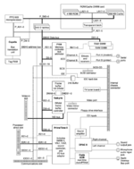
Even with buffers, the bandwidth is limited. But it does make me think: if you use the main DRAM as your read frame-buffer, then maybe you could improve the effective bandwidth. I did wonder at one point if you could use the L2 cache itself as the read frame-buffer, because 320x240 x 2 = 150KB, just over half the cache. However, the cache appears to be two-way set associative (see the Tag RAM bit of the diagram), so you'd have to use every other 32-byte block.
I saw this example code, and I think it is odd that I always see 168 cycles, given the dynamics. Maybe the context switch is substantial too.
I thought it might be a context switch issue. The 603 has banked GPR registers for handling TLB misses. I think it says there are 4 registers. Maybe Apple doesn't use Motorola's algorithm. Do you get 168 cycles on different versions of Mac OS?

Interesting, and fun!

-cheers from Julz
 
I'd still like to return to the idea that the chipset wasn't the problem. Here's some more of my reasoning:
  1. In the PC world, these things made no difference. It didn't matter if there was multiple graphics architectures: CGA/EGA/VGA(MGCA)/Hercules/SVGA and then later chipsets with increasing hardware support.
All of those standards had two things in common:
(a) they were, or somehow became, standard (!), so you could get them from multiple vendors, driving costs down
(b) as video standard, they were all (I think) "chunky color", dumb (no acceleration) direct-access framebuffers (same as Macs and most Unix workstations), i.e. super easy to use

The issue with the Amiga chipsets were
(1) bad call on the type of framebuffer (bit-planar vs. chunky)
(2) the directly accessible *acceleration* in the chipset from things like blitting, etc.

When using CGA/VGA/whatever on the PC, you'd go (sometimes) through the abstraction layer that is BIOS to get some basic parameters, wrote a few standard registers to setup the video mode, and then just blasted pixels in the framebuffer.

Early PC video card weren't accelerated at all, and wouldn't be (except for specific use cases) until Windows 3.x had a nice abstraction layer to add some 2D acceleration. A lot of if had been pioneered by the XWindows crowd (some remnants of which are visible in the EXA acceleration layer of Xorg) and the Mac (with QD acceleration). The applications didn't use those directly - they went through the abstraction layer (X server, QuickDraw, Windows <whatever>).

  1. In the PC world it didn't matter if they had to write directly to the hardware or use OS APIs or DirectX, it was still a success.
Writing directly to the framebuffer was never an issue, as it's mostly about computing an offset to a base address. Acceleration is the problem. It's the thing that ties the application to the hardware. Mac and PC didn't have any of that application-accessible until they had enough of (an) abstraction layer(s) in place, and in use. That is why they suceeded.

  1. In the Video console world it didn't much matter if they switched CPUs or had totally different graphics architectures: most consoles did really well (with the exception of the N64 or Sega Saturn and although Sega didn't seem to survive the Saturn failure, Nintendo did prosper after the N64).
Console don't care about backward compatibility; first they want to sell new games (where the money is), second the generations are sufficiently far apart than a new generation could reimplement/emulate an older one if backward compatibility was really needed. Sure, the 7800 was backward-compatible to the 2600, but that didn't exactly help. And it didn't help moving between nintendo, sega, sony, and microsoft during the 80s/90s.

  1. In the Mac world it didn't matter that the compact Macs had 1bpp x 512 x342, with no hardware assist, then the Mac II had indexed 8-bit graphics and subsequent Macs had increasing or varying hardware assist (which is part of the conversation about Valkyrie's pixel-doubling mode).
It very much did, as most games written for the 128/512/+ were broken on the Mac II, due to the 512x342/B&W assumption (and probably also assumption on the base address, that could vary depending on the slot used in the II).

Once the II was introduced, developer had a choice between (a) ignoring the II and targeting only B&W compacts (which some still did for games) (b) following apple guidelines to make it work on all possible configuration of the II. That second point saved the Mac - most applications went through the Toolbox, and were still running perfectly on the IIx, SE/30, IIcx, IIci, ...

Apple did not care about not selling II to gamers - they didn't want the Macintosh to be perceived as a game system, as the Apple II was still being sold and had already a lot of that market. Apple wanted a prosumer system. That decision probably help the macintosh a lot long-term, vs. the minimal lost sales short-term (the price of the II wasn't exactly that of a game system anyway).

  1. In the Acorn world it didn't matter that the Archimedes had almost no hardware acceleration and the platform had a tiny market share mostly confined to the UK, they still managed to keep the platform going longer than Commodore did.
Acorn had a captive market though education. Thomson sold a lot of computers in France for the same reason, and some were in use long past their relevance due to educational software on them. Ultimately Acorn didn't have much of an impact on the world of computer, except for that Risc Machine thingumajig :-)

  1. Even for games that exploited the Amiga hardware, many games were converted between the ST and Amiga, so developers would have abstracted much of the lower-level graphics functionality
And famously not ported to the Amiga, with Carmack being quite vocal about why. And port between ST and Amiga had a lot in common (identicle CPU optimization), and were mostly rewritten for the graphics part to adapt to each machine- I'd say the graphics part was isolated more than asbtracted... Something developers hated, because it costs a lot of money, and the further along the 80s and 90s the fewer machines games were ported on, until pretty much only the PC was left going through the BIOS/DOS/Windows abstraction layer(s).

What all of these platforms and the companies behind them had in common was that they cared about the platform and improved the hardware over time.
... with an abstraction later for backward compatibility, and occasional "pruning" of really old stuff (16-bits mode in Windows, OS9 stuff in OSX, ...). At least for those successful, which only includes PC, Mac, and not console (not backward compatibility) nor Acorn (commercial failure).

I figure if the Amiga had had worse graphics, it would have either gone the route of the Atari ST and died at a similar time, though arguably, the Amiga survived better thanks to third-party PPC boards and MorphOS.
It didn't survive. Commodore disappeared, and that was it. The fantasy of the Amiga crowd that it "survived" is just that, a fantasy. The amiga had zero (0) real-world relevance by then, and only had an ecosystem of accelerators and random PPC-based redesigns sold at extravagant price to a dwindling bunch of fans. The ST "survived" in the exact same way in Germany, even though the US didn't care much for it.

I don't know for right now, but some years ago people were still creating games for many 8-bits systems of the 80s. Doesn't mean they survived, either.

As I see it, the problem was really Commodore's lack of leadership. Despite considerable effort from engineers, they were more interested in milking the existing hardware than have a vision for the platform. They floundered trying to switch to PC computers, undermining confidence in the Amiga itself, much as Palm and Nokia did when it decided to switch to WinCE (or Windows Mobile as it probably had become).
Alternative view on the leadership: they realized that backward/binary compatibilty was the redeeming feature of the PC (and Mac), and were desperately trying to find alternative sources of revenue for the company as the writing was on the wall for their computer lines (C64, C128, Amiga). "milking the existing hardware" was needed to fund the next source of revenue...

The Apple II crowd was using similar argument to diss Apple lack of investment in the platform during the IIc and IIgs era. They couldn't see the platform was already dead either, and Apple had no choice but to find alternatives. They had the III and Lisa as complete failure. Unlike Commodore, they eventually found a platform that could carry them in the future with the Mac - though for a long time that wasn't obvious.

I think this ties to some previous comments as well: "normal" people (so not terminal geeks) buy a computer as a tool to run some software, and then moves on when it becomes obsolete/breaks down. Software is updated all the time, but not necessarily at exactly the same time as hardware, so you want some level of overlaps, hence the "normal" need for backward compatibility for a certain period of time. After a while, sufficiently old software "can" break, as the number of people who cares (like those with an early '09 MBP as their personal laptop...) has become low enough. Tying software to the hardware the way the Amiga did makes it a lot harder to have this cycle of co-evolution.
 
(I don't have a Sparc workstation, but I do have an SGI Indy with an R4000 and a HP-715 [or 735])
I have an SGI and a couple of HP-PA HPs somewhere, but I don't like them the way I like my SPARC. By now, the primary reasons is lack of documentation. Sun documented a lot of things very well, as they had to support clones, and they also pushed for standardization (SBus, SPARC itself). I was able to recreate a SBus device because all of it was very well documented, and some of the required tools (OpenBoot firmware in Forth, ...) are still available. I was able to "clone" some of the functions of the cg6/GX accelerated framebuffer because some of the architecture documents surfaced on bitsavers. Someone did manager to recreate a SS5-compatible system in a FPGA, capable of running vintage OSes. There's Xrender acceleration running on the cg14/SX in NetBSD because the hardware was sufficiently documented.

Most of the stuff from SGI and HP were fully proprietary, so there's very little you can do with them other than preserving them. None of the proprietary bus were documented, not any of the graphics device, etc. And I don't like that.
About a year back I had fun playing with the SparcStation emulator that could run Netscape 3.
I wanted to get the LCC compiler (rather than GCC) to run on SunOS 4 so I had a proper, but fairly light-weight ANSI 'C' compiler, but I got a bit stuck with the changes to the assembler (different directives for bss, data and const sections). I was trying to go down the normal cross-compiler route. I found a decent ANSI C to K&R 'C' converter (unproto from the bcc compiler. It's better than ansi2knr); then I was going to compiler LCC and its tools by using unproto first. Then I could recompile LCC directly using the pseudo-LCC.. but I didn't make all the changes to the code generator to work with the assembler, so that could never run.
 
Hi @Melkhior ,

Thanks for the extensive reply. So, in my replies I <snip> chunks out, not because they're unimportant, but simply to leave key words as reference points.
<snip> (a) <snip> standard (!) <snip> driving costs down.. (b) <snip> "chunky color" <snip> super easy to use. [vs] Amiga <snip> (1) bad call <snip> (bit-planar vs. chunky) <snip> accessible *acceleration* in the chipset <bigSnip> Mac and PC didn't have any of that<snip> until <snip> (an) abstraction layer(s) in place, and in use. That is why they suceeded.
Still not sure that's really the case. Let's consider the alternative: the Commodore Amiga & ST had chunked graphics instead of bit-planar. Both of these machines were well cheaper, at least at the A500/A600/ST-FM level than comparable PCs until basically after they failed. I was reading some BYTE issues from 1992 and found that even the cheap 386 PCs were still $1200+. PC standardisation didn't provide cheaper, better graphics (you could have one or the other). If these companies had gone for basic, chunked graphics, would they have lasted longer and been more popular?

I think not, because what made them competitive when they came out were the features you reason killed them in the end. With poorer graphics, they would have been replaced by PCs sooner. Don't you think?

And that's my underlying point: how could companies possibly compete with the PC, from the mid-80s onwards? So should they have even tried? People were surprised Apple even tried with the Mac instead of launching an Intel PC in 1984.

What would have been your strategy and why would it have worked better than Commodore's or Ataris?

Console don't care about backward compatibility<snip> most games written for the 128/512/+ were broken on the Mac II <snip>
Crystal Quest? Say it ain't So ;-) !
<snip>Apple did not care about not selling II to gamers <snip> Apple II was still being sold <snip> probably help the Macintosh <snip>
I think that's probably true.
Acorn <snip> education. Thomson <snip> same reason <snip> Ultimately Acorn didn't have much of an impact on the world of computer, except for that Risc Machine thingumajig :)
ARM :-) !
<snip>The fantasy of the Amiga crowd that it "survived" is just that, a fantasy<snip>
Though, a more active fantasy than the ST, I think that's all I was comparing it to.
<snip> but some years ago people were still creating games for many 8-bits systems of the 80s<snip>
Oh, they still are! This is also part of that thread, PM5200 on the demoscene ;-) !
Alternative view on the leadership: they realized that backward/binary compatibilty was the redeeming feature of the PC (and Mac)
Interesting, but from my experience of articles at the team and reading other blogs and articles, I don't think their leadership even reached that level of competence. Commodore's PC business even damaged them more than Amiga failures.
The Apple II crowd was using similar argument to diss Apple lack of investment in the platform during the IIc and IIgs era. They couldn't see<snip>
I think I read a bit about that. I was in the "Mac is obviously the future" crowd having experienced them since late 1986.
I think this ties to some previous comments as well: "normal" people (so not terminal geeks) buy a computer as a tool to run some software <snip> [Summary: technology overlap and rolling obsolescence].
Apple seems to handle that pretty well these days and to an extent the PC industry seems to be following suit, if less conscientiously: older PCs just get too slow to run the new stuff, and there's a faster churn.

Anyway, toodle-pip for now, thanks for the replies! Cheers from Julz
 
Hey Snial,

I checked a bit more in the manual for the 603. Let's first just ignore L2:

A cacheable read, that is not in L1, the following will happen:

1. cpu executes the load, the MMU will say it is cacheable, and that it is not in L1. So a cache burst read will be requested on the bus.

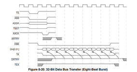
The bus transaction for a burst read can be seen in the 603 manual, 8.6.1 "32-bit data bus mode".
It says protocol is the same as in 64 bit mode, so the critical word should go first:
2024-08-11-180408_728x385_scrot.png

The 603 has a 32 bit address bus and a 64 bit data bus, in the figure we see what happens in both:
- TS (transfer start)
- ABB (address bus busy)
- ADDR (address 32 bits)
- TBST (transfer burst)
- AACK (address acknowledge)

2. Capella must be the one that acks the address and starts to talk to F108 to get first the critical word, and then the subsequent words, so Capella knows in which order these are coming in on the data bus, and on the 603 data bus the CPU sees the critical word and gives it directly to the execution unit(s) that needs it, and will also write the incoming words to L1.

As for timing: at best, after 4 bus cycles, the critical word is on the 64 bit bus, that is 16 cpu cycles (2:1 bus to cpu). But I see 32 cycles empirically. All this has a lot more details to it in the manual, and I feel I only have an "overview picture" (hopefully mostly correct), perhaps something in those details will add further delay.

Now it is somewhat of a mystery how the L2 cache makes sure it is updated as well as L1. Because as you pointed out, as the critical word comes in on the 64 bit data bus, the L2 only sees A17-5, so it would not know which offset the first word is at. It is also somewhat mysterious what the "P_D4-0" is for, why does it say D?

What would be reasonable, is that the L2 will be up to date with L1 and use the data that came on the data bus. I *think* that most likely, the diagram in the 5200 developer note is not giving us the full picture, and possibly the P_D4-0 is actually extra information for L2, only used when the burst read comes in when it missed in L2.

For the case when L2 hits, it is a little bit easier, because it would only sense that the 603 needs the block, and could send all the data on the 603 bus, but again, it would not know about the critical word so it would not know which word to put first, but by the 603 protocol, it must give the critical word first.

Clearly, there is some interaction here between the 603 bus and the L2 that we are missing the details on.


OK, I think that might make sense. P_A21-5 selects on 32 byte boundaries, but a 64-bit access is an 8-byte boundary, so we need to select one of 4 x 64-bit slots and that could be done via P_D4-0 from Capella... no that no longer makes sense again. It'd be better just to have P_A21-3 as the transparent latch.


I think it's possible to prove which way around it works by reading adjacent words. If the CPU reads the critical word directly from DRAM and then the rest of the cache line is filled, you'd find that there would be the 32 cycle delay reading the first word, but also a significant delay reading the following word as you'd have to wait for the rest of the cache line. However, if Capella fills the L2 cache, then releases the CPU bus to read the critical word from the L2 cache, then you'd find that the next word would be read in 1 or 2 cycles.

Even with buffers, the bandwidth is limited. But it does make me think: if you use the main DRAM as your read frame-buffer, then maybe you could improve the effective bandwidth. I did wonder at one point if you could use the L2 cache itself as the read frame-buffer, because 320x240 x 2 = 150KB, just over half the cache. However, the cache appears to be two-way set associative (see the Tag RAM bit of the diagram), so you'd have to use every other 32-byte block.
I'm not sure I understand the "tag RAM", would you help and explain that a bit and why that would indicate L2 being 2-way? (To me it seemed it was N-way based on the empirical data where there was no clear pattern showing e.g. only every other block being cached).

As for the DRAM read frame buffer, yes, this is on my "TODO" to investigate. It is quite a bit of trade off, because not writing to VRAM directly means you have to do it later, so you add overhead work, but you *might* gain it back. I've some ideas on how I might be able to make that work in a fast way, but would require several things to be put in place first.
 
Back
Top