Hi @noglin ,
I'll try and reply to the rest later, but just skipping ahead:
It's really very similar to what the L1 cache has: 8kB of content + 128x2 tags. The L2 cache stores 256kB of recently used DRAM (or VRAM) accesses. So, the L2 cache, like the L1 cache is divided into a number of 32-byte 'lines', i.e. blocks. Tag RAM determines which address range of DRAM is being tagged by a given line of cache, essentially it's a cache of the upper part of the address for that line. A direct mapped cache would simply need to check the top 32-5 = 27 address bits. But the index can just be checked directly, so the tag memory doesn't include that. So, the remainder is stored in RAM per tag entry and 256kB cache would need 256kB/32B = 8192 entries x (27-13 [because there's 13 bits that don't need to be checked as they're the tag entry]=14 bits), which itself is a fair amount, about 14kB in itself.
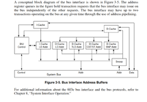
Every time Capella sees a bus request address. It indexes the tag ram using bits 5 to 21 (13 bits) of the address and if the tag bits match the upper 14 bits of the address, then the L2 cache line is correct and the 603 can read from the cache directly.
That's how it'd work for a direct-mapped 1x way cache. For a 2 way L2 cache we need an extra address bit because each L2 cache entry could come from 2 places (8192 entries x 15 bits). A 2-way cache would have better performance than the same sized 1x way cache. You'd need 1 more bit for the LRU, bumping it up to 31 bits for both entries. Capella would therefore have a 31-bit 'data' interface to the tag ram as it'd have to read both tags at the same time; then invert the LRU bit.
Your algorithm that goes sequentially through RAM would still see the same 32 cycle spike every 256kB. That's also the case for an LRU, N-way L2 cache, because the least recently used entry will always be 256kB ago.
I had an idea about how to avoid FDIV in an implementation of Quake. Quake has a limited horizon. Therefore, Z probably has a range between 1mm and 100m. So, storing a large 100,000 element array of 1/Z would provide up to 100m of range at a 1mm resolution, this reduces the problem to a memory fetch at the cost of 400kB (32-bit floats) or 800kB (64-bit floats). Anything further away, is going to be (a) very small and (b) easy to interpolate without needing an FDIV.
The second idea was to compute two 16-bit pixels and combine them in a single 32-bit word before storing the results. That way the two cycle store x 32-bits is equivalent to 2x 1 cycle stores x 16-bits each (though maybe packing the pixels would cost another cycle). Maybe, also, because we have 32 GPRs we can unroll loops a bit more than a Pentium could with its crummy 8 registers. 32 GPRs can store 64 x 16-bit pixels worth of data; 16 GPRs can store 32 pixels.
I'll try and reply to the rest later, but just skipping ahead:
I suspect it's not N-way, because that would need a lot of tag RAM.I'm not sure I understand the "tag RAM", would you help and explain that a bit and why that would indicate L2 being 2-way? (To me it seemed it was N-way based on the empirical data where there was no clear pattern showing e.g. only every other block being cached).
It's really very similar to what the L1 cache has: 8kB of content + 128x2 tags. The L2 cache stores 256kB of recently used DRAM (or VRAM) accesses. So, the L2 cache, like the L1 cache is divided into a number of 32-byte 'lines', i.e. blocks. Tag RAM determines which address range of DRAM is being tagged by a given line of cache, essentially it's a cache of the upper part of the address for that line. A direct mapped cache would simply need to check the top 32-5 = 27 address bits. But the index can just be checked directly, so the tag memory doesn't include that. So, the remainder is stored in RAM per tag entry and 256kB cache would need 256kB/32B = 8192 entries x (27-13 [because there's 13 bits that don't need to be checked as they're the tag entry]=14 bits), which itself is a fair amount, about 14kB in itself.
Every time Capella sees a bus request address. It indexes the tag ram using bits 5 to 21 (13 bits) of the address and if the tag bits match the upper 14 bits of the address, then the L2 cache line is correct and the 603 can read from the cache directly.
That's how it'd work for a direct-mapped 1x way cache. For a 2 way L2 cache we need an extra address bit because each L2 cache entry could come from 2 places (8192 entries x 15 bits). A 2-way cache would have better performance than the same sized 1x way cache. You'd need 1 more bit for the LRU, bumping it up to 31 bits for both entries. Capella would therefore have a 31-bit 'data' interface to the tag ram as it'd have to read both tags at the same time; then invert the LRU bit.
Your algorithm that goes sequentially through RAM would still see the same 32 cycle spike every 256kB. That's also the case for an LRU, N-way L2 cache, because the least recently used entry will always be 256kB ago.
Cool!As for the DRAM read frame buffer, yes, this is on my "TODO" to investigate. It is quite a bit of trade off, because not writing to VRAM directly means you have to do it later, so you add overhead work, but you *might* gain it back. I've some ideas on how I might be able to make that work in a fast way, but would require several things to be put in place first.
I had an idea about how to avoid FDIV in an implementation of Quake. Quake has a limited horizon. Therefore, Z probably has a range between 1mm and 100m. So, storing a large 100,000 element array of 1/Z would provide up to 100m of range at a 1mm resolution, this reduces the problem to a memory fetch at the cost of 400kB (32-bit floats) or 800kB (64-bit floats). Anything further away, is going to be (a) very small and (b) easy to interpolate without needing an FDIV.
The second idea was to compute two 16-bit pixels and combine them in a single 32-bit word before storing the results. That way the two cycle store x 32-bits is equivalent to 2x 1 cycle stores x 16-bits each (though maybe packing the pixels would cost another cycle). Maybe, also, because we have 32 GPRs we can unroll loops a bit more than a Pentium could with its crummy 8 registers. 32 GPRs can store 64 x 16-bit pixels worth of data; 16 GPRs can store 32 pixels.
Last edited:

") , I can tell you that I do use a LUT indeed, but it is *much* smaller, and uses some mathematical tricks to make it possible. One day I will document it, but I'll have to hold it a secret until I've made an even better demo for the 5200 as I actually have a competitor in this space
, I can tell you that I do use a LUT indeed, but it is *much* smaller, and uses some mathematical tricks to make it possible. One day I will document it, but I'll have to hold it a secret until I've made an even better demo for the 5200 as I actually have a competitor in this space  (which I am very happy that I do, way more fun when more people are trying to push the same hardware, actually, if you make a demo for the 5200 I will tell you the trick
 ")