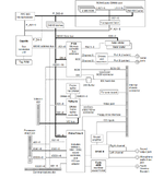
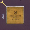
I keep returning to the M88K. Here's the MC88110 pinout:
96+65+72+8+49 signals=290 total.
The Vcc and GND pins don't really count as signals, in the PGA package they are through-hole so they connect directly to the power and ground planes - not routing needed. You do need to decouple them properly, though. Not much of a problem on a dual-sided board, but if you want a cheaper single-sided board you end up with this kind of monstrosity:

A row of 0402 capacitors both top and bottom in that socket window, and another three rows (!) both left and right. And some more on the outside. The bulk capacitors in the middle needs to be bigger (package) to account for derating, probably should be 1206 instead of 0603.
Signal-wise, I think this board has 106 actually connected in total; the many resistors surrounding the '110 are mostly pull-(up|down) to disable/hardwire some stuff (not all are done IIRC, haven't looked at that one in a while), and this wouldn't support SMP IIRC. Not finished because I don't think that one will ever happen. I would need to write a FSM on the FPGA for the '110 bus first anyway, and while the bus is a bit easier to handle than the 60x, it's already a lot tougher than the '030, '040 or '060. Also the motherboard for it is currently MIA has a critical component was obsoleted before I got around to even thinking of actually making one.
I think I'd also cut down the pin count. I'd only have a 32-bit data bus
Nah. Don't cripple the CPU, in particular if you also intend to reduce the caches' size. Honestly while the number of signals is bad if you want to connect everything to a FPGA on a cheap 4 layers board with not-too-expensive-connectors on a hobbyist's budget, for a mass-produced design in the eraly 90s it's not a deal-breaker. Anything post-MC68020 is using burst or similar to load full cache lines in normal use, so you want as fast and wide a bus as possible (a MC68020 only ever load 32-bits at once so a 32-bits bus is sufficient). I expect the '110 to be quite reliant on its fast bus for performance.
Not needed for personal computers, I agree (say the guy with ECC on his desktop...).
no transfer code (no FC equivalent)
Didn't connect them, don't think they are necessary (they are on the '020/'030 to talk to the FPU and other coprocessors, or to do some custom memory space like the Sun 3's control space in FC=3, but for a '040 or later it's not really useful anymore), so agreed.
; extra +5V and GND signals reduced proportionally.
You can get away with fewer for the data bus if you reduce the bus width (and a bit on the data/address but if you get rid of the parity), but other than that they are needed for the various parts of the CPU. You can probably get away with a lower number a lower frequency, but for proper power supply it's really tied to the silicon itself and where the power is needed/delivered.
The '110 EC document breaks down the power pins in each of the three domains (Internal Logic, External Signal and Busses, and Clock). For Vcc it's 40/25/1, for GND 45/27/1.
This gives: 64+45=109, with +5V and GND representing another 90% on top gives around 208 pins for a SQFP package down to 168 pins for a BGA (the same as an i486DX). The release date for the R41/25 was summer 1992 (3 years before the P5200) and updates allow it to scale to 75MHz + 64kB L2 cache before being replaced with the M88LC120/100MHz in Summer 1995.
The '110 package isn't that bad, and having a unique package for all variants would have been easier/cheaper. I believe (not sure as the design above is just a PoC) that a lot of the bus signals can be tied up/down for a cheap single-CPU implementation; the only thing they would have needed to do is a way to disable parity by firmware (which may or may not exist already, I can't remember what I was planning on that front other than maybe expand the card with a bunch of ACT11286 to compute appropriate parity locally).


 !
!