• Hello MLAers! We've re-enabled auto-approval for accounts. If you are still waiting on account approval, please check this thread for more information.

How did the PowerPC 603 / 5200 at 75mhz compare to PC:s (486/Pentium)?

Also interesting. I knew IBM compromised with Moto on the PowerPC by giving it the M88K bus interface, but I guess they also snuck in some of their own features too.
I believe so, because if you ignore the direct-store interface, the 60x bus is similar to the 88110 bus (the original 88100 is quite different as it has split instruction and data busses and pretty much need a pair of 88200 to make a conventional workstation).

There's some differences between the 88110 and 60x bus:
(a) the 60x parity is optional and also available on addresses (88110 has mandatory parity on data, none on addresses)
(b) transfer size is more versatile on the 60x ('110 does 1/2/4/8 bytes and 32-bytes burst, 60x can do all from 1 to 8 plus 32-bytes burst)
(c) there's some large differences in transfer attributes: the '110 transfer code (TC) signals are reminiscent of the '020/'030 Function Code (FC), while the 60x uses Transfer Type (TT) and Transfer Code (TC) that are completely different
(d) probably others I didn't notice/forgot (at least the UPA bits are gone, not that anybody really used them and the bits in the MMU are gone as well IIRC)

The 60x bus ends up needing even more pins than the 88110, though you can save on parity.
 
Interesting how experiences can vary so much. Then again @Snial thinks that the PowerBook 1400/117 is ‘just a bit lazy’, so he is obviously a patient man.
I really did laugh out load on that one :ROFLMAO: !

The actual quote is:

Mac OS 8.1 seems pretty lazy (but OK) on my PB 1400c/117
From:

https://68kmla.org/bb/index.php?thr...ternal-ide-hard-disk.45873/page-2#post-509662

Maybe I should buy a P630 at some point, Mac OS 8.0 is even more lazy on that (I had one briefly, to sell on).

I do have lazy Mac limits. I wouldn't run System 7.5.3 on an LC II or less. And for all my love of lazy Macs I haven't downgraded my PB1400c/166 back to 117MHz!

<snip> the 60x bus is similar to the 88110 bus
Sorry, I meant the single-chip version.
<snip> differences <snip> 88110 has mandatory parity on data <snip> transfer size is more versatile <snip> transfer attributes <snip> UPA bits are gone <snip> more pins.

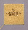
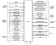
I keep returning to the M88K. Here's the MC88110 pinout:
1752934583499.png

96+65+72+8+49 signals=290 total. In my Fantasy M88K Macs thread, I talked about the NuMac R41/25, which has a fantasy cut-down 25MHz M88LC110 with 4kB code + 4kB data caches (instead of 8kB each). I think I'd also cut down the pin count. I'd only have a 32-bit data bus, no byte parity, no transfer code (no FC equivalent); extra +5V and GND signals reduced proportionally. This gives: 64+45=109, with +5V and GND representing another 90% on top gives around 208 pins for a SQFP package down to 168 pins for a BGA (the same as an i486DX). The release date for the R41/25 was summer 1992 (3 years before the P5200) and updates allow it to scale to 75MHz + 64kB L2 cache before being replaced with the M88LC120/100MHz in Summer 1995.
 
I keep returning to the M88K. Here's the MC88110 pinout:
96+65+72+8+49 signals=290 total.
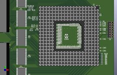
The Vcc and GND pins don't really count as signals, in the PGA package they are through-hole so they connect directly to the power and ground planes - not routing needed. You do need to decouple them properly, though. Not much of a problem on a dual-sided board, but if you want a cheaper single-sided board you end up with this kind of monstrosity:
CD_MC88110RC_50.jpg
A row of 0402 capacitors both top and bottom in that socket window, and another three rows (!) both left and right. And some more on the outside. The bulk capacitors in the middle needs to be bigger (package) to account for derating, probably should be 1206 instead of 0603.

Signal-wise, I think this board has 106 actually connected in total; the many resistors surrounding the '110 are mostly pull-(up|down) to disable/hardwire some stuff (not all are done IIRC, haven't looked at that one in a while), and this wouldn't support SMP IIRC. Not finished because I don't think that one will ever happen. I would need to write a FSM on the FPGA for the '110 bus first anyway, and while the bus is a bit easier to handle than the 60x, it's already a lot tougher than the '030, '040 or '060. Also the motherboard for it is currently MIA has a critical component was obsoleted before I got around to even thinking of actually making one.

I think I'd also cut down the pin count. I'd only have a 32-bit data bus
Nah. Don't cripple the CPU, in particular if you also intend to reduce the caches' size. Honestly while the number of signals is bad if you want to connect everything to a FPGA on a cheap 4 layers board with not-too-expensive-connectors on a hobbyist's budget, for a mass-produced design in the eraly 90s it's not a deal-breaker. Anything post-MC68020 is using burst or similar to load full cache lines in normal use, so you want as fast and wide a bus as possible (a MC68020 only ever load 32-bits at once so a 32-bits bus is sufficient). I expect the '110 to be quite reliant on its fast bus for performance.

no byte parity,
Not needed for personal computers, I agree (say the guy with ECC on his desktop...).

no transfer code (no FC equivalent)
Didn't connect them, don't think they are necessary (they are on the '020/'030 to talk to the FPU and other coprocessors, or to do some custom memory space like the Sun 3's control space in FC=3, but for a '040 or later it's not really useful anymore), so agreed.

; extra +5V and GND signals reduced proportionally.
You can get away with fewer for the data bus if you reduce the bus width (and a bit on the data/address but if you get rid of the parity), but other than that they are needed for the various parts of the CPU. You can probably get away with a lower number a lower frequency, but for proper power supply it's really tied to the silicon itself and where the power is needed/delivered.

The '110 EC document breaks down the power pins in each of the three domains (Internal Logic, External Signal and Busses, and Clock). For Vcc it's 40/25/1, for GND 45/27/1.

This gives: 64+45=109, with +5V and GND representing another 90% on top gives around 208 pins for a SQFP package down to 168 pins for a BGA (the same as an i486DX). The release date for the R41/25 was summer 1992 (3 years before the P5200) and updates allow it to scale to 75MHz + 64kB L2 cache before being replaced with the M88LC120/100MHz in Summer 1995.
The '110 package isn't that bad, and having a unique package for all variants would have been easier/cheaper. I believe (not sure as the design above is just a PoC) that a lot of the bus signals can be tied up/down for a cheap single-CPU implementation; the only thing they would have needed to do is a way to disable parity by firmware (which may or may not exist already, I can't remember what I was planning on that front other than maybe expand the card with a bunch of ACT11286 to compute appropriate parity locally).
 
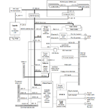
@Melkhior I have to take the opportunity and paste photos of the logic board, in case you would be interested in settling some questions we've been having reading the developer notes 😅

All notes says it is a 64 bit databus between L2 and CPU, so we think that is the case. We are not sure why capella is connected directly with "P_D0-4" to the 603 data bus.. is it really and if so why? And the "critical word" is supposed to be sent first, but L2 (and ROM) seems only connected to send full blocks (does not have individual addressing).
 

Attachments

Last edited:
Not a helpful contribution but the 5200 was the worst computer and or Mac I have ever owned. What a piece of crap.
That is a helpful contribution :ROFLMAO: but in what way was it the worst? Slow? or broke down? I've read many that had various hardware issues with it, but mine had none of those issues, it was working very well, and I really enjoyed coding on it while having the built-in TV with a small window next to the Think Pascal IDE (and later CodeWarrior with C). But for gaming.. well yeah it felt really slow.
 
The Vcc and GND pins don't really count as signals,
To preempt the rest of this. Gosh, you've made an incredibly informative response to my back-of-the-envelope+software-guy-ignorance post, so I'd just like to say thanks.

in the PGA <snip> through-hole <snip> - no routing needed. You do need to decouple them properly, though.
Didn't think of that, but good point.
<snip> 0402 capacitors <snip - locations and other caps as needed>.
Makes sense.
<snip> need to write a FSM on the FPGA for the '110 bus first anyway <snip>
I wanna backup a bit here. Is this an FPGA to manage a real MC88110, or an FPGA implementing an MC88110? I'll come back to this in a bit.
Nah. Don't cripple the CPU..
In a retro project built today I wouldn't. Imagining an early 1990s student's Mac built around an MC88110 I'm not sure they wouldn't, in order to cut costs. If Gary Davidian's LC-based RLC, must have had a 32-bit bus as it used an actual LC's ROM, would be twice as wide as an LC's 16-bit bus and I'm not sure any Macs in the 1992 era had a 64-bit data bus. But I'm happy to be wrong, perhaps Apple would have used a 64-bit bus even then.
in particular if you also intend to reduce the caches' size.
I was making estimates of the cost of the CPU: it would have about 500K transistors (MC88110 had 700K-800K didn't it?). I did some estimates of the performance of 4kB caches in my Fantasy M88K thread. The goal of the low-end NuMac 41 would be to provide LC II type performance for emulated code and better than a typical i486 for specialised math libraries and routines. The thinking is that by launching M88K Macs a couple of years earlier than actual PPC Macs; software (OS/Compilers/Mixed-Mode) support would be far less complete and therefore less ready to replace 68K Macs. Instead, they're used for more specialist applications while the late '030s/'040s carry the platform; and to prime students or developers over 1992 to 1995 until M88K Macs are properly ready.
<snip> FPGA on a cheap 4 layers board with not-too-expensive-connectors on a hobbyist's budget, for a mass-produced design in the early 90s it's not a deal-breaker.
OK. I was thinking at one point if someone was to create an FPGA-based MC88110, then it wouldn't even need to have exactly the same architecture. As long as it has behaviourally equivalent caches and can execute the Instruction set with the same kind of performance, then a much more simpler design should be possible, especially given it is a RISC.
Not needed for personal computers, I agree (say the guy with ECC on his desktop...).
Irony!

having a unique (i.e. shared) package for all variants would have been easier/cheaper.
True.
I can't remember what I was planning on that front other than maybe expand the card with a bunch of ACT11286 to compute appropriate parity locally).
An recreated MC88K Mac would be pretty interesting.
 
Last edited:
I wanna backup a bit here. Is this an FPGA to manage a real MC88110, or an FPGA implementing an MC88110? I'll come back to this in a bit.
As you noted later in your post, it's connecting a FPGA to a '110. Re-creating a '110 would be even more complex than recreating a full '030, and we still don't have that as open-source gateware :-(

The original idea was to create a FPGA-based motherboard with a CPU daughtercard (or two), and have the daughtercards be able to support more than one kind of CPU. Nothing else would be connected to the CPU (the FPGA handles everything, memory and peripherals alike, even if memory latency will be bad), so pinouts from the CPU to the connector can be somewhat arbitrary (but are split in "bussed" that are shared between the two daughtercard, and "dedicated" with a dedicated set of pins per CPU for e.g. bus arbitration signals and the like). I ended up drafting for the '030, both kind of '040 (V and non-V, as V despite lacking the FPU are much nicer to deal with as they are 3V3 and don't require the two clocks), '060 and '110. I wanted non-Motorola stuff, but ultimately there isn't that many 32-bits CPU with MMU running NetBSD (or at least a working toolchain) that can be sourced today... Also, it could be fun to try to get SMP support on the '030/'040/'060, even though the performance would suck (except maybe the '060).
 
My sister had a 5200 as well. It was slow, it froze all the time. Worst computer or Mac ever.

I recently got my 6200 back from my sister that I gave her, like, 25 years ago when she was working on a website and wanted a Mac so she could make sure her design looked good on Macs too (only Mac she ever owned). Not exactly the same as a 5200, but close enough.

I booted it up because it had been so long and I wanted to see if it was as bad as I remember, and it really wasn’t. That said, it’s defnitely my slowest PowerMac and I won’t be holding on to it.

Depends on the version of the OS you are using and if you are using the Connectix 68k emulator or Apple’s. Apple’s 68k emulator cannot fit in the cache of any NuBus-based machine. You can replace it with the Connectix emulator and have major speedups. I think it’s Speed Doubler that has it as part of its package. Later versions of Classic have a lot more PowerPC code, and with MacOS 8.6 Apple upgraded their “kernel” and it was PPC-based.

NuBus-based Performas also should not have their network serial line used. Doing so causes a lot of problems with other systems. This is all because with the 6200 Apple basically created a PowerPC 620 with the upgrade card built in. The 6300 has a few hardware improvements and the faster versions use the improved 603e that make those machines much better.
 
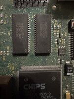
I'm adding a small piece of information here: the vram is 2x 512kb, and from the photo I took, it is NEC 424260, here is the datasheet for it:


I suspect that valkyrie chip hardwires one chip (512kb) for the the video buffers (320x240x2 bytes * 2 are in one), and the screen buffer is hardwired to the other (e.g. 800*600*8, 640*480*2). That would explain why it cannot do 1024x768 despite having 1MB, and also why there is no hardware backbuffer screen buffer even in 640x480x8. And possibly also why they decided to hardcode the base address (or so it seems, the driver I disassembled seems to read it hardcoded from rom and for sure never writes that address to any hw register in the driver)
OK I had to check the motherboard, and OK I can debunk my previous suspicion...
The A0-A8 seems to be connected between the two chips.

So valkyrie does 32bit read/writes by writing to same address to both chips and placing 2 bytes in one and 2 bytes in the other.
We know valkyrie has 8 buffered entries, the cpu read/writes to those, and that for video out these chips will be read, 640x480x8 + 320x240x2, at 60hz= 43mb/s.

And on top of vidoe out, we want to write to vram during vbl, that means 640x480x8bit*60hz = 17.5mb/s
(which I painfully know it struggles to do)

The bandwidth of these two chips are way higher than ~60mb/s from what I can tell?

Valkyrie should have had more entries in its buffer for the PPC.. as cpu vram writes are capped at about 17mb/s (when doing sustained writes)

I'm starting to think that Valkyrie really is the bottleneck for graphics on this machine, still hoping for some discovery to make it possible to do something that is competitive with the Pentium 75 but vram writes are a pain...
 

Attachments

So valkyrie does 32bit read/writes by writing to same address to both chips and placing 2 bytes in one and 2 bytes in the other.
We know valkyrie has 8 buffered entries, the cpu read/writes to those, and that for video out these chips will be read, 640x480x8 + 320x240x2, at 60hz= 43mb/s.
correction: valkyrie has 4 buffered transactions (e.g. 8 pixels in 16bit).
 
Back
Top