• Hello MLAers! We've re-enabled auto-approval for accounts. If you are still waiting on account approval, please check this thread for more information.

Is an inverter bi-directional: 74LS04 specifically?

Trash80toHP_Mini

NIGHT STALKER
68040
Need some general Digital Logic help here, gang.

None of the datasheets say whether the 04 inverts a signal going both ways. The arrow shape in the graphic tells me no and my gut tells me it must be an "understood" kinda deal that inverting a signal is a one way street? EVERY hit I get for bi-directional inverter is either another useless data sheet or worse, info on bi-directional AC/DC Inverters.

I REALLY need some help here, color me clueless/confused/concerned. :blink:

@Bolle is asleep and this one will keep me awake, so:

View attachment 27664

Those arrows look ominous and have for some time.

Here's the first bit of digital logic gibberish Bolle tossed my way:

View attachment 27536

This is Bolle's schematic in Greek as far as I'm concerned. But even after 45 years of corrosion from disuse, I'm probably still a little bit better at reading Greek than schematic.

View attachment 27670

My major concern is that we've got the LC PDS -> 030 PDS figured out, but there's either a disconnect or a wrong connection going from back to the NIC from 030 PDS -> LC PDS?

My heebiejeebies tell me we need the other three inverters on the way back to the NIC and diodes to direct the two opposing lanes of traffic? But I know next to nothing about digital logic. It looks like a bunch of pipe, valves, a whackdoodle silt collector cyclone/mixing valve thingie that needs backflow prevention valves in some mixed up section of my digitally impaired analog visual cortex. I don't think what I use for a brain will ever transition to digital. Fluidic logic I can "see" digital  .  .  .

HELP!!!! 8-o

 
Last edited by a moderator:
Shortest answer: no.

Followup: why in the world do you think it would need to be here? I haven't been following the other thread particularly closely but my vague understanding of what this inverter is for is to change the address at which some hardware on the peripheral card you have there will "wake up". Unless this peripheral is going to be doing bus mastering it's always going to be the computer driving the address bus lines so... again, why would you need the inverter to be bidirectional? 

 
Thanks! That's what I thought.

As I understand it, the inverter has the NIC filling memory locations in $A or $9 space instead of the stomping on the memory space of the SE/30 video subsystem at $E as it would be doing without one line being inverted for $A or all three inverted for $9.

When the SE/30 needs to feed data to the NIC, it's controlling the address lines, no? From the wiring of the inverter as is, I see none of those three address lines making a return trip over any wire to the NIC. I see a disconnect when the Jumper Blocks are configured to send the Address signals through the inverter on a one way trip. I see no connection back to the NIC for any of those three address lines. The NIC still thinks it's in $E and the SE/30 will be thinking it's at $9 or $A. I'm thinking those three lines from 030 PDS -> NIC need to be provided at best and inverted on the way at worst. The diode check valve thing is the only way I can describe controlling the flow of traffic on the ingoing and outgoing lanes.

My heebejebies are about the missing return leg on the journey of those three address lines to the NIC? Is something missing as is or am I missing something here?

edit: maybe I've got it backwards? trag was helping me a bit, but he'a really busy at work. He said we shouldn't assume the outgoing leg of the inverter was tri-stated as null. That's why I cut it completely out of circuit when not in use in my diagram. From the non-mastering point of view, does Bolle's initial diagram do the trick in both directions?

 
Last edited by a moderator:
Well... as Gorgonops said we don’t have to worry about the other direction unless we want to use a bus master card.

It‘s the host machine setting up the address lines all the time. The card latches in that address and presents whatever data it has on that address on a read from the card or waits for a strobe signal to read in data from the host bus on a write to the card. Those are the only two scenarios that should be happening on a non-busmaster card.

If we want to support bus mastering it would be easiest to do this with some programmable logic.

Have the address lines as feedback pins and monitor the R/W line as well as /BGACK to see if the card is in control of the bus. Address signals get inverted in both directions then and tri-stated accordingly if not used using OE conditions.

 
OK, thanks guys. This stuff is still clear as Koine Greek, but at least I can go to sleep now.

Is my "blocks of four" jumper setup for the inverter good to go as is?

 
Heading off to bed, but one more thing befor I let this embarrassment slide into oblivion: Bus Mastering on the SE/30! :lol:

 
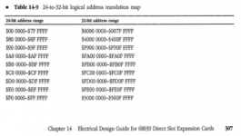
This is me being ignorant about the exact machinations going on in the parent thread again, and also probably ignorant about the requirements of PDS card re: 24 and 32 bit mode, but I'm going to toss this out there: I see you're putting inverters on the A20, A21, and A22 because you want to munge $A0 0000  into $90 0000. (Or was it vice versa? Whatever, it's not important.) Are you *sure* that's what you want to be doing? Here is why I ask, from page 307 of "DCaDftMF, 2nd ed.":

image.png

IE, it was my vaguest of understandings that in a Macintosh a card didn't really need to worry its head about whether it was running in 24 vs. 32 bit mode, the hardware was always designed for the 16MB "normal" Slot spaces at F9xx:xxxx to $FExx:xxxx and the PMMU (or that simpler mapper unit that was in the Mac II and the original LC) was used to remap the first 1MB of that normal slot space into the 24 bit slice.

*IF* that gibberish I said above is true wouldn't it follow that messing with the A20-A22 address lines would at best be unnecessary and at worst be deeply counterproductive? I dunno, maybe I'm totally missing something here.

 
My specific thought was in reference to the middle diagram that jt posted above.    It wasn't clear to me whether the red wires or the blue wires were meant to be input/output.

Case 1:  If the blue wire was in, and the red wire was out, then one could get the inverted address by putting a jumper on 2-3.   However, if one wanted the uninverted address, putting a jumper on 1-2 would get you a mix of the uninverted address and whatever the floating inverter happened to be outputting.

Case 2:  If the blue wire is out and the red wire is in, this works much better.   Now the uninverted address is available on pin 1 of the jumper.  The inverted address is available on pin 3 of the jumper.  One connects the output line, pin 2 of the jumper, to either pin 1 or pin 3 to obtain either the uninverted or the inverted address, respectively.     The problem  with this diagram is that, as far as I can tell, it is using the inverteres on the 7404 backwards.    In other words, pin 1 is connected to the output of the inverter.  Pin 3 is connected to the input of the inverter.

So, I don't think either case works, but I think Case 2 is the better choice if one just reverses which pins of the 7404 pins 1 & 3 of the jumper connect to.

 
Case 1:  If the blue wire was in, and the red wire was out, then one could get the inverted address by putting a jumper on 2-3.   However, if one wanted the uninverted address, putting a jumper on 1-2 would get you a mix of the uninverted address and whatever the floating inverter happened to be outputting.
That is a really good point. You're far better off leaving the output waving in the wind when the jumper's not being used than the input.

I still stand by my suggestion that this whole thing might be on the wrong set of address lines in the first place, but I might also be on crack for saying that.

 
Dunno about any of this crap, obviously, but this is what's set up on the board. Gut tells me I may need to swap input/output sources for the inverters, but like I said  .  .  .

View attachment 27693

Using two pairs of jumpers for each line I take the inverter entirely out of circuit instead of worrying about signals swaying in the breeze from whichever direction.

-  four shorting blocks installed as shown sets the board up for $A memory ops (need to set a block in the diagram for the IRQ to Slot $A as well)

-  changing orientation and adding another pair of blocks sets it up for $9 memory ops

-  three in a row straight across the top sends all address lines straight thu, kicking $E Video ops in the groin, but we gotta test it. [}:)]

Just need to know if I need to reverse the inputs/outputs before I start to wrap.

 
This is me being ignorant about the exact machinations going on in the parent thread again, and also probably ignorant about the requirements of PDS card re: 24 and 32 bit mode, but I'm going to toss this out there: I see you're putting inverters on the A20, A21, and A22 because you want to munge $A0 0000  into $90 0000. (Or was it vice versa? Whatever, it's not important.) Are you *sure* that's what you want to be doing?
I can help a bit there: we've set aside any possible 32 bit addressing considerations for the time being. We'll be testing for bare function in the SE/30 in 24-bit mode only.

The NIC thinks it's at $E00 0000 - whatever and inverting A22 dumps it over into thinking it's in $A00 0000 - whatever. Invert all three lines and shazzam, it's supposed act like it's in $900 0000 - whatever. That just happens to be the IIsi NuBus Adapter Slot ID, which I thought might somehow be magical. ::)

So switching from Slot E space to Slot A space is the requirement. Further decoding to include the Slot 9 space gambit was to keep me happy in my superstitious, blissful ignorance. :blink:

edit: technically the NIC isn't thinking anything, I know, but that's the way I could get it into words. Acting in a way that works  .  .  .  nevermind.

 
Last edited by a moderator:
can help a bit there: we've set aside any possible 32 bit addressing considerations for the time being. We'll be testing for bare function in the SE/30 in 24-bit mode only.
My point is that I'm not entirely convinced you are hitting the correct address lines. The Apple manual reads an awful lot like the MMU takes care of presenting a 24 bit view of the 32 bit normal slot space, that you don't need to have two separate sets of decode on the card. And if that is actually true then inverters on A20-22 are not going to change the address decoding in a useful way. To modify the 16MB slot space you should be playing with A24-26. And worse, if you really think there is going to be a problem with a conflict in 32bit mode you can't get away with ignoring it because it also reads to me like during hardware initialization it's going to be in 32 bit mode when it's looking for declaration ROMs, etc, regardless of what the control panel setting for the OS is.

I also got the distinct feeling looking at the third edition of the "Designing..." Manual's LC PDS section that there are some wrinkles about how chip select works for LC PDS that are different enough from 030 PDS that you're going to need to address them too. (You did notice how the LC PDS is missing A28-30, right?) But, hey, maybe I have no idea.

 
My point is that I'm not entirely convinced you are hitting the correct address lines.
Got that, just wanted to let you know where we thought we were coming from.

Those are some nasty problems.

I also got the distinct feeling looking at the third edition of the "Designing..." Manual's LC PDS section that there are some wrinkles about how chip select works for LC PDS  .  .  .
Yep, I thought even more were missing. I dumbed my LCIII 030 PDS to 68030 IIsi PDS graphic down for this insanity. I thought even more were missing from the 020 LC PDS, but apparently I missed that.

What's nagged me all along was the notation that /SLOTIRQ.E acts like NMRQ on NuBus Macs. Doesn't sound at all SE/30 tolerant. Found it, it's at the bottom.

View attachment 26863

Sorry about the editing, I hit quote and everything went downhill from there. :-/

 
Last edited by a moderator:
My point is that I'm not entirely convinced you are hitting the correct address lines. The Apple manual reads an awful lot like the MMU takes care of presenting a 24 bit view of the 32 bit normal slot space, that you don't need to have two separate sets of decode on the card. And if that is actually true then inverters on A20-22 are not going to change the address decoding in a useful way. To modify the 16MB slot space you should be playing with A24-26. And worse, if you really think there is going to be a problem with a conflict in 32bit mode you can't get away with ignoring it because it also reads to me like during hardware initialization it's going to be in 32 bit mode when it's looking for declaration ROMs, etc, regardless of what the control panel setting for the OS is.

I also got the distinct feeling looking at the third edition of the "Designing..." Manual's LC PDS section that there are some wrinkles about how chip select works for LC PDS that are different enough from 030 PDS that you're going to need to address them too. (You did notice how the LC PDS is missing A28-30, right?) But, hey, maybe I have no idea.


The presented addresses differ in 24 and 32bit mode on the LC. Verified that in the other thread (why do we have two now anyways?)

Solution on how to handle 24/32bit mode switches to fool the LCPDS CS decoders are there as well. You’re right, A28-30 are involved... we basically need another address decoder to decode the full address. /FC3 is used on the LCPDS to compensate for the missing address lines.

 
Last edited by a moderator:
That doesn't read the way I meant it, sorry, G. What I meant to imply was that every time I see you answer simply, sigh, take it a step back and expand upon the fallacy of my thinking I learn a crap ton of new and interesting stuff. Thank you.

 
@Bolle having the technical side of the other thread break out into a serious discussion here is serendipity in action.

The IP of the other thread advertises it as the shot in the dark in need of hardware experimentation that it is, just to see what happens. The wire wrap discussion probably should be kept a tangential offshoot of this new, meaningful, main line of technical discussion.

@Gorgonops what I meant when I said I missed the point you made about the missing address lines was that I was surprised to go back and find it to be only three lines on the LCIII extension of the LC PDS.

Here's the PCB rats nest diagram I dumbed down to LC PDS spec. Visual differentiation of LC and LCIII connections to the 030 PDS may be helpful here.

View attachment 12609

My question at this point would stem from "the Macintosh Way" of doing things outlined in DCaD manuals:

Assuming the NuBus version of the card pre-dates introduction of the LC by some time or that the two cards were developed simultaneously, which amounts to the same thing:

NuBus card design would have been transferred wholesale to the PDS card. When that is assumed to be the case

-  hardware adaptation would be handled on the card itself within a module in its ASIC?

-  In true 128k wizardry fashion, following DCaD guidelines the same basic driver would be used for both versions of the NIC

-  NuBus NIC version would be communicating though the multiplexed NuBus using the full set of control lines

-  LC NIC driver would be communicating through the more limited 020 PDS using the subset of control lines available

-  LC PDS version would have a table conversion module appended to baseline driver for

-  CPU would be communicating with the formula infested ASIC on the NIC

-  ASIC degibberized control signals would be handed off within the ASIC

The same general purpose hardware on either NIC would be behaving in the same manner, one from NuBus MUX, the other from 020 PDS MUX. WAG from the origins of the other thread was that the NuBus driver would make conversion of the LC NIC possible.

WAG now is that the conversion has already been done, including 24/32 bit complications in the hardware/driver combination on the NIC/Floppy combo @maceffects sent my way.

The trick here is to make sure the LC driver can run on the SE/30 CPU to take care of everything BUT the memory mapping. The 030 PDS "CPU" is already in LC PDS speak mode in 24/32 over available subset of control lines on the left side of the LC/LCIII divide above?

There that's out of my system, now where's the obvious fallacy in that logic?

 
Now that I've stopped trying to think in .TXT above and poured a bowl of cereal: outlandish WAG of the day

Address inversion in hardware isn't necessary, just the IRQ line jumper? We've been thinking hardware hack when the crux of the matter would hacking the LC NIC driver to talk in $A memory mapping as opposed to its native $E memory mapping while it's hooked up by the IRQ line for $A? It's already in LC speak mode when it comes to hardware on both sides outside of that pesky IRQ line?

 
The presented addresses differ in 24 and 32bit mode on the LC. Verified that in the other thread (why do we have two now anyways?)
Okay, if it's verified then I guess you know what you're doing. (I tried looking for specific discussion of that in the other thread, I really did, and honestly I just couldn't follow it through all the interstitial pictures of wiring looms. Maybe I need more coffee.) I'll just note one last time that my concerns are based on passages like this: (Page 133 of D..3rd ed:)
 

As explained in Inside MaCintosh, a Macintosh computer operates in either 32-bit or 24-bit mode. In 32-bit mode, it can access all the address space in both the standard slot and super slot spaces of any slot card. In 24-bit mode, it can address only 1 MB of each card's standard slot space. This first megabyte of standard slot space is called minor slot space. In 24-bit mode, the computer hardware translates 24-bit addresses of the form $sx xxxx into 32-bit addresses of the form $FsOx xxxx, where s is a digit in the range $9 through $E.


Addresses of the form $Fssx xxxx access the same NuBus slot in both 24-bit and 32-bit modes. However, if you use an address of this form in 24-bit mode, the system will translate it into a NuBus address of $FsOx xxxx. In 32-bit mode it will remain unchanged. Hence, if you need less than 1 MB of address space to be accessible from NuBus, you should design your card to use only bits /AD19-/ADO. By ignoring bits /AD23-/AD20, you guarantee that addresses of the form $Fssx xxxx will be valid in both 24-bit and 32-bit modes.
This *is* in the NuBus section of the manual, but there are passages in the PDS section (that I think I've quoted before) that made me think that this translation still happens with PDS cards. But, hey, if I'm wrong I'm wrong. Do you have a reference that shows PDS cards actually need to decode both the standard *and* minor slot spaces?
 

Solution on how to handle 24/32bit mode switches to fool the LCPDS CS decoders are there as well. You’re right, A28-30 are involved... we basically need another address decoder to decode the full address. /FC3 is used on the LCPDS to compensate for the missing address lines.


I assume the A28-A30 decoding issue is why you have the PLD in there. Are the "A22LC" and "A26" outputs from that chip essentially what's going to be used for device enable for the LC card?

 
Last edited by a moderator:
Back
Top