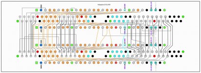
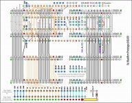
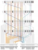
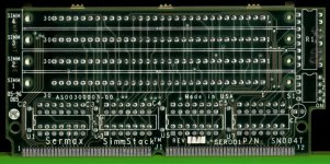
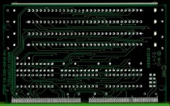
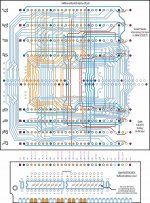
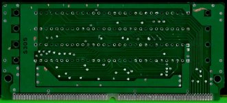
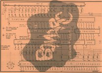
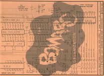
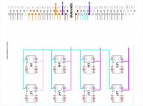
OK, I've finally got the first prototype worked out! Maybe . . . :blink: Simplified view of traces on both sides of a 10x10 PCB:

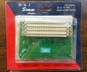
Decided I should make provision for adding line drivers (245s) and maybe the resistor packs found on higher quality SIMM savers. So I'm back to using dummy SIMM cards and a header/socket interface with 245s on at least one pair of risers. I'll definitely test without drivers or resistors first. The taller B & C versions of my Type D adapter may have pretty long traces.

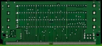
Dunno, we'll see. Broke one of the SIMM sockets taking my Type D apart to scan the component side, so I'll have to tear up another cheapo board for parts.
Still need to replicate the mirrored Power/Ground planes and I'll probably add a triplet of vias on all lines heading into and out of the 72pin SIMM socket for easily drilling out the center and soldering patch wires for any corrections to the outer vias. I hate cutting traces. You can see the vias to be drilled out for installing the line drivers and they'll be added for cutting any redundant connections to the mobo.
Does anyone have any idea why there are traces leading to n.c. positions? They're in brown. Very curious, they don't appear to be going anywhere?
Makers seem to have laid out data lines any which way to get the board down to two layers. I suppose it doesn't matter where the bits wind up, so long as everything's consistent. Colors got messed up a bit somewhere between AI, PDF and JPG export, I'm tired, but it's good enough for a look see.
Any suggestions? Corrections? Anything?
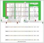
edit: looks like the address buses on the Verification test SIMM sockets didn't get copied over to the single layer file. It's a lot prettier when it's fully symmetrical tracewise, if not in connector spacing. Oopsie! :-/
