-
 Hello Guest! We're hosting a challenge to welcome vintage Intel macs to the MLA during the month of July! See this thread for more information.
 -
We've made some quality of life improvements to the Trading Post. More info here.
You are using an out of date browser. It may not display this or other websites correctly.
You should upgrade or use an alternative browser.
You should upgrade or use an alternative browser.
SE/30 Overclock: Is it possible?
- Thread starter EvieSigma
- Start date
I'm fairly certain with the SE/30 that's a flat no, because unlike some later systems it uses a single oscillator to derive all the clocks in the system. (IE, you change that and you'll foul up the video timing, scsi, everything.) Therefore to make it run any faster you need to add some circuitry to allow the cpu run asynchronously.
But that's just a half-memory, I could be wrong.
But that's just a half-memory, I could be wrong.

That, and I'd imagine that overclocking a compact Mac would be dicey anyway because of heat-dissipation issues.
Totally doable, and possible. You will need to replace the Crystal for the XTAL frequency on the CPU. I believe (Correct me if I'm wrong) the CPU runs at a 1:1 ratio with the XTAL source.
Problem is I don't know what's going to happen to whatever else derives their signals from that clock. Usually the first things that break is ADB/Serial and possibly SCSI.
ALTHOUGH, I have an idea that you can leave that Crystal in place so all of the system devices keep their stock clock, but then setup the higher frequency crystal ONLY for the XTAL input to the CPU. So you could cut the XTAL pin that comes from the old crystal, and run it to the new one. That way the CPU is overclocked, and nothing else breaks.
Edit* Totally doable, pin E1 gets routed to the XTAL of the higher frequency crystal.
Last edited by a moderator:
Here's a thread on doing it. By cutting some traces and piggybacking a second crystal for ADB and Serial it's possible to sorta get it working, but:
#1: the floppy drive won't work
#2: Sound will be messed up
#3: You'll have to use a video card like a Micron Exceed because the internal video timing will be utterly fouled up.
In short, yes, it's sort of possible if you're willing to butcher your motherboard, but I kind of think that's beyond the scope of what the OP wants to do.
Last edited by a moderator:
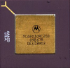
That 68030 is socketed in the SE/30 isn't it? If it is, you could easily do it without anything crazy in a number of ways. It would only be snipping one pin either way, or insulating it.
Off the top of my head I'm reasonably sure that just feeding a different clock signal into the CPU without adding any arbitration logic isn't going to produce particularly good results. (And how you plan to do this without either cutting a trace, which is a spotty proposition on a multi-layer board, or interposing some sort of sandwich board between the CPU and the socket is, I guess, an exercise for the reader.) My ignorant reading of the 68030 application manual suggests that at least some of the signals between the CPU and the bus controller are synchronous, IE, you can't just dump a different clock into the CLK signal pin and expect things to magically work without some logic to line up the timing. So far as I know no commercial accelerators consist of just a crystal dumping into the clock pin, they all have arbitration logic.
Have you actually done what you're suggesting?
Have you actually done what you're suggesting?
Of course not, but if we lived by that logic we would still be in caves.Have you actually done what you're suggesting?
I read that article you posted, as you can see for the most part that actually worked. Keep in mind, he changed the Crystal for the entire system. Most of those problems wouldn't prevail if we went my suggested route and added a second Crystal directly for the CPU..
As far as I can tell, he might be okay if he doesn't go too far with the CPU clock as there possibly could be something with that GLU to do with the problems the others had. I think you're talking about the MC88916 that'd be in charge of all the BUS signals. Only thing I'd be concerned about at this point is the 68882. How that FPU is going to handle that deviation from stock clock is anyone's guess. I'm thinking you'd have to pull both the FPU and CPU to that new Crystal. I don't have the schematics so I cannot really make anything for certain, really a shot in the dark. But it'd be worth a shot.
In terms of actual implementation you'd just need to run a fine wire loop around Pin E1, and run that to the newer Crystal. Then go ahead and cover the Pin itself with some electrical tape or Krylon if you have any. That will insulate the old Source in the socket, and connect it to the new one without a drop of solder (although, you'd want to make that permanent after testing). Then you can at least give it a shot. Nobody is guaranteeing it's going to work, but that's part of the fun. Might work, might not.
Last edited by a moderator:
No, cavemen don't have access to Motorola's manuals and application notes. It's worth pointing out that there's a lot more in those than the chip pinout. Cutting a trace on motherboard with no idea what will happen is what a caveman does.Of course not, but if we lived by that logic we would still be in caves.
Overclocking the entire system like that breaks those peripherals, sure, but it also clocks all the CPU's communication to the bus and memory controller up by the same amount. The 68030 has no less than *16* pins relating to bus arbitration and supports both synchronous and asynchronous operation and without deep reading of those manuals referenced above *and* a look at the SE/30 schematics I can't say if just slapping a clock which is completely out of phase with the bus clock will work at all, and if it does how badly it'll work. (Things like pulse width and such are important, there are timing diagrams in said manuals.)I read that article you posted, as you can see for the most part that actually worked. Keep in mind, he changed the Crystal for the entire system. Most of those problems wouldn't prevail if we went my suggested route and added a second Crystal directly for the CPU.. .
Do you have any idea how tightly the pins in a PGA package like a 68030 fit the socket? It takes earth-shattering force to pull one of those things out of their socket and it's about as bad a task to shove it back in. There's no way you're wrapping tape around a pin to insulate it from the socket, and in fact I have serious doubts you'd even be able to manage it if you tried painting the pin with an insulating coating; socket will scrape it right off.In terms of actual implementation you'd just need to run a fine wire loop around Pin E1, and run that to the newer Crystal. Then go ahead and cover the Pin itself with some electrical tape or Krylon if you have any.
(Also, not very many SE/30s have socketed CPUs in the first place, but I suppose if we're going to handwave hard enough that's no big matter either.)
Last edited by a moderator:
There's no real reason to have more than one crystal in a compact. The only reason you'd need a second clock in something like the IIcx (very near fraternal twin of the SE/30) would be for implementing the 10MHz NuBus clock. SE/30 doesn't need that because the PDS runs at the CPU/System clock. Both systems date from a couple of years before split buses at the system level hit the Mac (or PC?) world.

the 020 and better most bus transactions are async. So increasing the CPU speed shouldn't affect anything, because it will add additional bus wait states via the DTACK line. I have already researched all of this.
However 68000 backwards compatibility does require an E-clock which IS synchronous and drives the VIA, SCC, etc.. But on an SE/30, this is all handled by the GLU and is not by the CPU anymore. CPU handles the address calls asynchronously and the GLU does the rest internally.
You can cut the clock line to the CPU, and build an ICS511 circuit to double the clock speed to 33Mhz while keeping it phase-locked to the rest of the system.
But again, its going to insert additional wait states so the performance gain? Not much unless it has on-chip cache.
In theory you could stick an 030 in there running at 100Mhz, but you wouldnt see any speed increase. Why? Well... its still talking to RAM at a blazing sped of 16/33mhz.
True acceleration requires the RAM, Shadowed ROM, cache to be the same width, and running at the same speed as the accelerated CPU to gain any kind of performance.
Then some sort of logic, or reprogrammed MMU to select "your" ram instead of "that" RAM.
RAM and ROM have to sit in the same memory mapped position on the bus as the original RAM and ROM, but to stop bus contention, it has to be figured out that when the system selects RAM memory addressing, it doesnt call back to the logic board, but to the accelerator instead. Same thing with ROM. Only way this is possible is by hijacking the address decoding, and the only way to do that without seriously hacking the hardware is remapping via an MMU.
Last edited by a moderator:
What I was curious about was this: the suggestion made here was essentially to cut the CPU clock completely off from any phase association with the rest of the system and just freerun based on a completely divorced crystal. (Which of course means that the relationship between its internal timing and the bus is both completely unpredictable and prone to drifting randomly over time.) I've not done more than skim the 68030 reference manual and while section 7.2.8 covering asynchronous bus operation does say is supports being used in that manner there still seem to be areas that would be affected by the timing relationship between the two being "completely random". (For instance, time window limitations on when and how long the DSACK* lines can be asserted, etc. There's also some verbage in the in-depth descriptions for the asynchronous read/write cycles that further make me wonder what havoc might be wreaked if the clocks were to end up badly out of phase.)You can cut the clock line to the CPU, and build an ICS511 circuit to double the clock speed to 33Mhz while keeping it phase-locked to the rest of the system.
I dunno, *shrug*, maybe it would work, depending on how tolerant the bus controller will be to said out-of-phase clocks causing lines to be asserted at "weird" times, but that's only assuming the SE/30 *never* uses synchronous transfers for anything. Maybe it doesn't, I have vague memories of looking at that during a discussion of how fast in theory an SE/30 could transfer data to RAM in a PDS video card, but is there a definitive answer to that in the SE/30's publicly available documentation?
I dont think you can go over 2 to 4x. because there is a timing window on how many wait states can be inserted before the BERR fires.
In a minority of them it is - most of them seem to be soldered down. It's pot luck which one you get.That 68030 is socketed in the SE/30 isn't it?
Similar threads
- Replies
- 10
- Views
- 3K
- Replies
- 0
- Views
- 223
- Replies
- 8
- Views
- 2K
- Replies
- 1
- Views
- 257