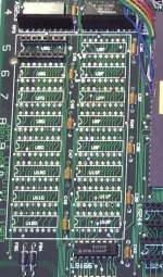
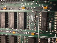
I have a 512k that the ram went bad and recently de soldered the ram. Whenever i try to re solder it it won't stick. I fluxed the board. But it still wont work.
You are using an out of date browser. It may not display this or other websites correctly.
You should upgrade or use an alternative browser.
You should upgrade or use an alternative browser.
Re soldering the ram on a 512k
- Thread starter Macintoshguy1984
- Start date
looks the same. How could i fix this.
It looks like you might have popped out some of the via's when you were desoldering. :-/
Obv its a bit hard to tell with the glare, but you could always see if you could solder down 2 points to hold down the ram and reconnect it manually
with 30-32 awg wire, because its only a 16 pin dip so you'll not even have to do that much work.
Obv its a bit hard to tell with the glare, but you could always see if you could solder down 2 points to hold down the ram and reconnect it manually
with 30-32 awg wire, because its only a 16 pin dip so you'll not even have to do that much work.
I'm a little confused by the scorch marks on the upper surface on the board. How were you doing the desoldering, with a wick? Also, did you use force to rip the chip lose?
Personally, since my soldering skills suck, I'm a big believer in snipping off the legs and removing them with a solder sucker. (Often I use the technique of suspending the board vertically so I can apply heat to the pin on the solder side with the sucker pressed in place on the other side of the hole, ready to slurp as soon as things start to move.) Unless I really want to try to save the IC it's *so* much easier than trying to get the all X pins clean enough to let go gently at once.
Personally, since my soldering skills suck, I'm a big believer in snipping off the legs and removing them with a solder sucker. (Often I use the technique of suspending the board vertically so I can apply heat to the pin on the solder side with the sucker pressed in place on the other side of the hole, ready to slurp as soon as things start to move.) Unless I really want to try to save the IC it's *so* much easier than trying to get the all X pins clean enough to let go gently at once.
Gorgonops method is good. I have found another good method with DIPs is to turn the board upside down, support it about an inch off the bench and wave hot air around on it until a pointy instrument (like dental picks)says the solder is soft, then gently push the pins out and let the chip fall out. Don't try to pry it out from the front. This method is especially good if you might wish to reuse or test the chip in question.
I did what Gorgonops did but I ripped out the chips with a pair of pliers after de soldering
Uhm, yeah. If you "ripped them out with pliers" they were by definition not completely desoldered.
(Also, I'm confused: what I do is cut the legs off the chips with angle snips *before* I desolder them, IE, the chip itself is gone before I remove the solder and pins, preferably in one go, with the sucker. There's no "ripping" involved.)
(Also, I'm confused: what I do is cut the legs off the chips with angle snips *before* I desolder them, IE, the chip itself is gone before I remove the solder and pins, preferably in one go, with the sucker. There's no "ripping" involved.)
Honestly, with the level of damage to this board the best suggestion I'd have for trying to fix it would be to piggyback replacement chips onto adjacent chips in the same row... tack down all pins but... 2 and 14, it looks like according to the datasheet? to the legs of the chip below, and then using fine wire run jumpers to where the traces that used to go to those pins on the destroyed sockets terminated. Only reason I can think of that wouldn't work is if in the process of yanking out the vias you broke connections to chips further down the line.
(Each bank of 8 chips is wired in parallel other than the read and write pins, the aforementioned pins 2 and 14. One end of that parallel grid is going to be connected to things like the power supply and address generation circuitry, and it's very possible when you yanked out and destroyed the copper pads you broke the lines to chips further down the same row. If that's the case then on the backside of the board you'll have to patch *more* jumpers around the breaks.)
The end result would look terrible but it might get the board running.
Could you show me a picture of that
Ram piggybacking? Well, here:

Here's an illustration of the basic technique, although what you'd want to do in your case is a little different. What the person has done here is stacked a second 4116 DRAM chip on top of each of a set of 8 chips, soldering all the pins in parallel except for one of the control lines; the pin for that one is bent out straight and then they're all wired together with jumpers (as you can see in the picture) and sent to an output generated by address generation circuitry (either already present or added) that enables the new chips when it's appropriate.
Since in your case you're not trying to add new memory it's not the control circuitry you not to want be in parallel, but the data in/out lines. (The Mac only accesses memory in byte/word size chunks so all the chips in a given back of RAM will be enabled at the same time.) So what you would do is bend up lines 2 and 14 (assuming I got that correct earlier, might want to double check it) on however many chips you need to replace the memory in the spaces you destroyed, solder all the remaining pins to the legs of chips in adjoining positions, solder jumper wires to the "Flying pins", and then solder the other ends of those jumpers to where the lines that ran to pins 2 and 14 of the chips you're replacing ran to. (Can't tell you that without a detailed schematic or squinting at the real circuit board and tracing the traces.)
In principle this should work fine because all the control and address lines going to all the RAM sockets are in parallel anyway, it's *just* the data bits that go to unique destinations for each chip. In practice your board might still not work, because the extent of the damage you did in ripping the old chips off might have broken the parallel wiring. To determine whether or not that's the case you'll have to check continuity across the address and control bus from end to end. If you do find breaks you might be able to fix them by adding *yet more* wire jumpers to bridge the gaps. Try to keep everything neat, this is basically the most timing-critical area on the whole motherboard and crosstalk and noise from sloppiness *will* cause problems.
Where are the address and control bus? And where could I find a diagram of the macintosh motherboard? Finally, what are the 2 wires i need to solder
Last edited by a moderator:
That's a really good question. There are detailed full schematics for the Mac Plus floating around but all that easily turns up on a search for schematics for the original models is this "cheat sheet" diagram that may be perfectly fine for a troubleshooting tech to use but if you're groping around in the dark it's not going to help you a whole lot. Frankly I think you're going to have to have this damaged motherboard in front of you and noodle it out. Use a continuity tester (most multimeters have a "beep" setting built in now for that) to double-check what you trace with your eyes.And where could I find a diagram of the macintosh motherboard?
Because *I* don't have a mac motherboard sitting in front of me there are limits to the precision of the things I can tell you.
Here is a datasheet for the type of RAMs used in the Mac 512k Look at the pinout for the 16 pin DIP package of this type of RAM. Pins 1, 5-7, and 9-13 compose the multiplexed address bus, while pins 3, 4, and 15 are the "control" pins that orchestrate the multiplexing of the address bus, refresh, and when data is to be read from or written to the chip. Here is a clip from a picture I scrounged up a Mac motherboard that's had all its RAM removed to install an upgrade that hangs directly off the CPU socket and whatnot, showing the traces between the RAM chips:Where are the address and control bus?

This is actually a really useful picture because it shows pretty clearly that all of those pins are tied together in each row of sockets. Also, helpfully enough, notice that pins 2 and 14, which are the "D" and "Q" pins, IE, "Data In" and "Data Out" pins, are *not* tied together, so unless they are on the other side of the board that supports my conclusion that those are the correct pins to require jumpers.
As I said earlier, to try this you'll take pins #2 and #14 on each chip you're going to add to replace the RAM you ripped out and *carefully* bend those legs of the chips up and out of the way to when you stack the chip on the one below they won't touch the corresponding pin. Then you will press the chip in on top of the one already on the board and tack each remaining leg to the one below it. Here's roughly what it'll look like, in this case in a chip not already soldered down:Finally, what are the 2 wires i need to solder

*Then* what you will do is solder wire jumpers to the pins you bent up and out of the way (or maybe you'll want to do this first, just make sure to make the jumpers long enough to go where they have to), and then you will route those jumpers in such a way that they connect to the destinations those pins *used* to connect to on the IC areas you destroyed. Here's a photo of the non-component side of a Mac motherboard but I totally do not have the patience to follow the traces and figure out where the best place for you to run those wires to is. You *could* try running them to the holes for pin 2 and 14 in the holes you mangled, gluing them down on the component side, and then seeing dumping enough solder into place gets you a working connection to the end of the trace, but my guess is you'll be better off following the trace to the next VIA or IC pin it terminates at and anchoring it there on the component side.
AND AGAIN, I HAVE TO REITERATE: Look at the picture I put in above that shows how the traces for the control lines are all wired in parallel, and notice how each socket's trace comes from the contact point of the last socket. You didn't post a picture of your whole board showing which positions you mangled, but there's a really good chance you damaged connectivity to any sockets "downstream" of the ones you worked on, which means the control bus will be incomplete and you'll have to fix that *too*. You can do that by tacking jumper wires between the matching IC legs/solder pads of either side of the holes you made. You can *check* to see how bad the situation is with your continuity tester by sticking it against the aforementioned control bus pins (IE, basically everything except numbers 2 and 14) at one end of each line of chips and touching the matching pin on every chip in the row. If you don't get a beep you've got something to fix.
Similar threads
- Replies
- 24
- Views
- 2K
- Replies
- 11
- Views
- 1K


