Sweet! [ ] ]'> Glad you finally went public with this avenue of investigation. Rock on! [
 ] ]'>
] ]'>
You are using an out of date browser. It may not display this or other websites correctly.
You should upgrade or use an alternative browser.
You should upgrade or use an alternative browser.
ProtoCache1 - IIsi/SE/30 PowerCache Adapter Prototype Development
- Thread starter Trash80toHP_Mini
- Start date
Attached is the full equation dump of the DualPort IIsi adapter.  The dream is nearly complete!
Name DualPort IIsi;
PartNo 00;
Date 8/5/2017;
Revision 01;
Designer Joe Carter;
Company 68KMLA.ORG;
Assembly None;
Location U2;
Device virtual;
/* Dedicated input pins */
pin 1 = I0; /* Input */
pin 2 = I1; /* Input */
pin 3 = I2; /* Input */
pin 4 = I3; /* Input */
pin 5 = I4; /* Input */
pin 6 = I5; /* Input */
pin 7 = I6; /* Input */
pin 8 = I7; /* Input */
pin 9 = I8; /* Input */
pin 11 = I9; /* Input */
/* Programmable output pins */
pin 12 = B0; /* Combinatorial output */
pin 13 = B1; /* Combinatorial output */
pin 14 = B2; /* Combinatorial output */
pin 15 = B3; /* Fixed high output */
pin 16 = B4; /* Fixed high output */
pin 17 = B5; /* Fixed high output w/ output enable */
pin 18 = B6; /* Combinatorial output */
pin 19 = B7; /* Fixed high output */
/* Output equations */
B7 = 'b'1;
!B6 = !I5;
B5 = 'b'1;
B4 = 'b'1;
B3 = 'b'1;
!B2 = !I2 & !I9;
!B1 = !I6 & !I7 & !I8;
B0 = I0 & !I9;
/* Output enable equations */
!B5.oe = !I0 & !I1 & !I2 & !I3 & !I4 & I5 & I6 & I7 & I8 & I9 & !B0 & !B1 & B2 & !B3 & !B4 & !B6 & !B7
# !I0 & !I1 & !I2 & !I3 & !I4 & I5 & !I6 & I7 & !I8 & !I9 & !B0 & B1 & B2 & !B3 & !B4 & !B6 & !B7
# !I0 & !I1 & !I2 & !I3 & !I4 & I5 & I6 & I7 & !I8 & !I9 & !B0 & B1 & B2 & !B3 & !B4 & !B6 & !B7
# !I0 & !I1 & !I2 & !I3 & !I4 & I5 & !I6 & I7 & I8 & !I9 & B0 & B1 & B2 & !B3 & !B4 & !B6 & !B7;
/* End */
Next step is to compile the functions into a JEDEC fusemap and burn it to a new ATF16V8. I'll then place the copy in my socketed DualPort IIsi and make sure it works. After that, we can work on getting a prototype card built.
Last edited by a moderator:
Ah ha! Very nice! Grayscale whoop whoop!
Your avatar needs updating with an eye patch and a parrot if you're going to be springing any more treasures from this haul on us! Woot!
Yeah, it's been quite an adventure. Unfortunately, my programmer can't handle the latest (and only available) revision of the ATF16V8C, so I had to source some old Lattice GAL16V8s. It'll be a little while before I receive them to test.
Fabulous progress! :approve:
Is the I/O pinout listing for the GAL on the previous page complete? All other signals are a straight thru bus from MB to PDS via the crazy detours through CI, the IIci Cache Slot's oddball, one off pinout?
Is the I/O pinout listing for the GAL on the previous page complete? All other signals are a straight thru bus from MB to PDS via the crazy detours through CI, the IIci Cache Slot's oddball, one off pinout?
Yeah, pretty much that's complete, other than missing pin17 and pin18, which I have now detailed below. I still need to verify this with a complete blind re-check, and compare those results with these to be certain. I will do that whilst I await my new PALs.
But yeah, pretty much all signaling is connected 1:1:1:1 between the PDS30, THRU, CACHE, and FPU slots, where they exist. I wouldn't really call it a detour through the CI, because you have to think of it as a shared bus between all the connectors, rather than an origination or end point. It's more like a rubber stamp application of an assertion all at once rather than piping that propagates through subsystems.
However, there are these important exceptions:
BGACK
The BGACK signal from PDS30 is connected to the PAL, pin 12. It is connected 1:1 between the THRU and CACHE slots, but also held high through a 122Ω to +5V, and also connected to the PAL, pin1. It is not a valid FPU signal, so it is absent there.
R/W
This signal is connected 1:1:1:1 between all four slots, but also connected to the PAL, pin2.
BG
/BG from the PDS30 is connected to the PAL, pin3. It is connected 1:1 between the THRU and CACHE slots, also connected to the PAL, pin14. It is not a valid FPU signal, so it is absent at the FPU.
DS
This signal is connected 1:1:1:1 between all four slots, but also connected to the PAL, pin4.
RSVD
This is a mystery signal derived from pin A1 on the PDS30 slot. It's function is currently unknown. This signal is connected 1:1 between the PDS30 and THRU slots, but also connected to the PAL, pin5. It is not a valid signal on the CACHE or FPU slots, so obviously absent at those locations.
RESET
The /RESET signal is connected 1:1:1:1 between all four slots, but also held high through a 391Ω resistor to +5V. It is also connected to the PAL, pin6.
A0
The /A0 signal is connected 1:1:1 between the PDS30, THRU, and CACHE slots. It is not connected to the FPU. Instead, A0 is connected to +5V at the FPU. I thought that strange. Why would /A0 would be connected to +5V and only at the FPU slot? Well, after reading the 68882 user manual, I find that /A0 (along with /SIZE) is used to set the FPU operation mode. If both signals are low, the FPU runs with an 8-bit data bus. If both are high, it runs with a 32-bit data bus. And if /A0 is low, and /SIZE is high, it runs with a 16-bit data bus. So that explains this anomaly quite well!
A1
The /A1 signal is connected 1:1:1:1 between all four slots, but also connected to the PAL, pin8.
A4
The /A4 signal is connected 1:1:1:1 between all four slots, but also connected to the PAL, pin9
CPUDIS
This signal is only valid on the CACHE slot. It is held low with a 122Ω resistor to GND. It is also connected to the PAL, pin11
D0
This signal is connected 1:1:1:1 between all four slots, but also connected to the PAL, pin15.
D3
This signal is connected 1:1:1:1 between all four slots, but also connected to the PAL, pin16.
CENABLE
This signal is only valid on the CACHE slot. It is connected to the PAL, pin17.
CFLUSH
This signal is only valid on the CACHE slot. It is connected to the PAL, pin18.
BERR
/BERR is connected 1:1:1 between the PDS30, THRU, and CACHE slots. It's not a valid FPU signal, so it is absent there. It is also held high through a 681Ω resistor to +5V.
CACHE
This one is a bit odd, but I toned it out several times to be sure. Pin B2 on the PDS30 slot is identified as GND in the DCaDftMF. And indeed, on the PDS30 slot, it is tied to GND. However, on the THRU slot, it is not connected to GND. Instead it is connected to the CACHE B40 pin, identified as the /CACHE signal. I'm trying to figure out why this would be, but let me assure you, it is.
HALT
HALT is connected 1:1:1 between PDS30, THRU, and CACHE slots. It is not a valid FPU signal, so it is absent there. However, these signals are also held high through 681Ω resistor to +5V.
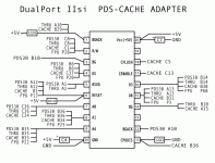
I created this diagram to help visualize the connections and their relationship with the PAL:
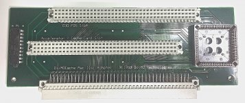
I've been thinking about making one of toledogeek's Quick and Dirty flexable PDS extenders, but with a CACHE slot on the end and my PAL wired in. Sure, I'd lose the PDS passTHRU, but it'd be a quick proof of concept to see if everything is in order.
But yeah, pretty much all signaling is connected 1:1:1:1 between the PDS30, THRU, CACHE, and FPU slots, where they exist. I wouldn't really call it a detour through the CI, because you have to think of it as a shared bus between all the connectors, rather than an origination or end point. It's more like a rubber stamp application of an assertion all at once rather than piping that propagates through subsystems.
However, there are these important exceptions:
BGACK
The BGACK signal from PDS30 is connected to the PAL, pin 12. It is connected 1:1 between the THRU and CACHE slots, but also held high through a 122Ω to +5V, and also connected to the PAL, pin1. It is not a valid FPU signal, so it is absent there.
R/W
This signal is connected 1:1:1:1 between all four slots, but also connected to the PAL, pin2.
BG
/BG from the PDS30 is connected to the PAL, pin3. It is connected 1:1 between the THRU and CACHE slots, also connected to the PAL, pin14. It is not a valid FPU signal, so it is absent at the FPU.
DS
This signal is connected 1:1:1:1 between all four slots, but also connected to the PAL, pin4.
RSVD
This is a mystery signal derived from pin A1 on the PDS30 slot. It's function is currently unknown. This signal is connected 1:1 between the PDS30 and THRU slots, but also connected to the PAL, pin5. It is not a valid signal on the CACHE or FPU slots, so obviously absent at those locations.
RESET
The /RESET signal is connected 1:1:1:1 between all four slots, but also held high through a 391Ω resistor to +5V. It is also connected to the PAL, pin6.
A0
The /A0 signal is connected 1:1:1 between the PDS30, THRU, and CACHE slots. It is not connected to the FPU. Instead, A0 is connected to +5V at the FPU. I thought that strange. Why would /A0 would be connected to +5V and only at the FPU slot? Well, after reading the 68882 user manual, I find that /A0 (along with /SIZE) is used to set the FPU operation mode. If both signals are low, the FPU runs with an 8-bit data bus. If both are high, it runs with a 32-bit data bus. And if /A0 is low, and /SIZE is high, it runs with a 16-bit data bus. So that explains this anomaly quite well!
A1
The /A1 signal is connected 1:1:1:1 between all four slots, but also connected to the PAL, pin8.
A4
The /A4 signal is connected 1:1:1:1 between all four slots, but also connected to the PAL, pin9
CPUDIS
This signal is only valid on the CACHE slot. It is held low with a 122Ω resistor to GND. It is also connected to the PAL, pin11
D0
This signal is connected 1:1:1:1 between all four slots, but also connected to the PAL, pin15.
D3
This signal is connected 1:1:1:1 between all four slots, but also connected to the PAL, pin16.
CENABLE
This signal is only valid on the CACHE slot. It is connected to the PAL, pin17.
CFLUSH
This signal is only valid on the CACHE slot. It is connected to the PAL, pin18.
BERR
/BERR is connected 1:1:1 between the PDS30, THRU, and CACHE slots. It's not a valid FPU signal, so it is absent there. It is also held high through a 681Ω resistor to +5V.
CACHE
This one is a bit odd, but I toned it out several times to be sure. Pin B2 on the PDS30 slot is identified as GND in the DCaDftMF. And indeed, on the PDS30 slot, it is tied to GND. However, on the THRU slot, it is not connected to GND. Instead it is connected to the CACHE B40 pin, identified as the /CACHE signal. I'm trying to figure out why this would be, but let me assure you, it is.
HALT
HALT is connected 1:1:1 between PDS30, THRU, and CACHE slots. It is not a valid FPU signal, so it is absent there. However, these signals are also held high through 681Ω resistor to +5V.
I created this diagram to help visualize the connections and their relationship with the PAL:

I've been thinking about making one of toledogeek's Quick and Dirty flexable PDS extenders, but with a CACHE slot on the end and my PAL wired in. Sure, I'd lose the PDS passTHRU, but it'd be a quick proof of concept to see if everything is in order.
Hi...i am a new user here. In my case i wanted to mount two 601 cpu's via cpi's and two pds boards and one nubus. I know I will probably have to upgrade or replace my PSU. According to Daystar's marketing material the Turbo 601 was supposed to work in the SE/30 so I'm hoping the 6100's will too. Will we have a choice in what we order?
This board would be to fit a single IIci CACHE slot style accelerator in an SE/30, and have a PDS pass through as well. Since it is basically a clone of the single PAL style DayStar card, whatever accelerators which work with that should work with this. It will in no way provide a NuBus slot, or a way to use accelerators which are not of the IIci CACHE persuasion.
I do wonder if a card could be designed to provide two PDS slots and one IIci CACHE slot. Iffy, because we rapidly loose space in the SE/30.
Perhaps two versions could be made. A short one for mounting on top an ethernet adapter (modified with a wrong angle adapter), and another proper height version.
When this project is complete, the equations for PALs will be public domain, along with the pinouts of the slots, so anyone can design a card which fits their needs, and burn the GAL to support it.
Some progress, and a hiccup...
I FINALLY successfully burned a Lattice GAL16V8D to replace the original MMI PAL16L8. It works, kind of... The accelerator functions, but if anything is plugged into the PDS passthrough, it causes no boot and definitely no fun. It works with the original PAL, so I know it is not a power supply issue. Besides, I'm using an ATX power supply so I should have endless amps for multiple cards.
I need to check the voltages coming into the GAL and refer to the datasheets. The Lattice part might have different input tolerances and output levels than the original MMI PAL part. I may need to play with different resistor values.
Next steps:
Figure out why PDS passthrough is a show stopper.
Decide if I should use the old style GAL or switch to a modern and readily available FPGA such as the ICE40 series.
Start designing a board.
I was recently thinking about this baed on Gamba's multi-PDS page, as I removed my ethernet to fit in the Micron card. Dual PDS would be stellar.I do wonder if a card could be designed to provide two PDS slots and one IIci CACHE slot.
Welcome aboard!Hi...i am a new user here. In my case i wanted to mount two 601 cpu's via cpi's and two pds boards and one nubus.
LOL! Been there, tried that. Another of my impossible dreams would be Project30.
NuBus on the SE/30 ought to be possible, the problem appears to be with how Bus Mastering Cards are handled on the its PDS. "Not well" or not as well as the IIsi, IIRC. The other gotcha is address mapping and Video memory conflict as in IIci adaptation for both SE/30 and IIsi. Someone with the chops to take a serious whack at that windmill (as zomb has done here) will need to get involved. I just set 'em up, don't have the expertise to actually do most of the projects I try to get rolling.
Takers? [
That ought to be doable, but the problem there is the limits of the PDS itself. The SE/30 is spec'd to drive just two inputs on the PDS, so line drivers/buffering will need to be designed and provided for on the adapter.I was recently thinking about this baed on Gamba's multi-PDS page, as I removed my ethernet to fit in the Micron card. Dual PDS would be stellar.
WAG: that'd be the other reason none of the Cache Accelerator Adapter mfr's provided a second passthru, Power limitations would be the first. ATX or booster pack required. :-/
It's a little more complicated than that. The output enable equation listed there is actually dependent on the Pin13 (B1) output which is fed internally in the PAL and used in the .oe. What you see listed up there is the raw decompile from pa, and can't be used to recompile without replacement/reduction with the internally used equations. I thought I had done this correctly, but perhaps not.
I've been plugging your equations (B0->B7) into the OE case in various ways to try and simplify it, but the end result is always a "true" or a "false". Unless there's more to it you're not showing, I don't see how this is working.
Edit: Without substitution that oe equation simplifies down to:
Not trying to get down on your work, I just like having something that can be reproduced easily
Edit: Without substitution that oe equation simplifies down to:
Its clear to see that when the equations you need to substitute are:out= B0&I6 +B0&!I8 +B1&I9 +B3 +B4 +B6 +B7 +I0 +I1 +I2 +I3 +I4 +!B0&I8&!I9 +!B1&!I6 +!B1&!I8 +!B2 +!I5 +!I7;
And if B7 = 1 and the output relies on B7, what should be my conclusion.... :-/B7 = 'b'1; /*eqns d'mgnd for simplicity*/
B6 = I5;
B5 = 'b'1;
B4 = 'b'1;
B3 = 'b'1;
B2 = I2 # I9;
B1 = I6 # I7 # I8;
B0 = I0 & !I9;
Not trying to get down on your work, I just like having something that can be reproduced easily
Last edited by a moderator:
I will post my strategy concerning the .oe for you when I get home, perhaps a second set of eyes can help out. Keep in mind, this is my first foray into PLD decoding, so don't think that I am a professional in any sense of the word. 
And also keep in mind, it isn't working yet. Hence, the black screen of nothingness when a PDS is installed.
Edit: Also, I don't think the output relies on B7. Pin19 is unconnected on the circuit board, and is always high. (which is practice, to keep levels from floating).
And also keep in mind, it isn't working yet. Hence, the black screen of nothingness when a PDS is installed.
Edit: Also, I don't think the output relies on B7. Pin19 is unconnected on the circuit board, and is always high. (which is practice, to keep levels from floating).
Last edited by a moderator:
Similar threads
- Replies
- 70
- Views
- 20K
- Replies
- 65
- Views
- 13K
- Replies
- 2
- Views
- 1K
- Replies
- 4
- Views
- 1K

