
I understand that, school is often keeping me from many of my electronics and car projects, glad to hear you might be able to get it working, I am still trying to round up cells for my DuosSorry to sounds like a broken record on this and the battery, but no. Been slammed with too many other priorities. Hoping to spend some time on it this weekend. It's a long-shot, but based on that hint from the dev note, I'm still hoping there might be a way to signal to the Duo that a serial modem is installed and bypass the software Hayes emulation layer. The guts of my poor 280c are strewn about my office, taunting me, judging me for my indifference and inaction. It's time to wrap it up I suppose...
-
 Hello Guest! We're hosting a challenge to welcome vintage Intel macs to the MLA during the month of July! See this thread for more information.
 -
We've made some quality of life improvements to the Trading Post. More info here.
You are using an out of date browser. It may not display this or other websites correctly.
You should upgrade or use an alternative browser.
You should upgrade or use an alternative browser.
PowerBook Duo Wifi Modem
- Thread starter sutekh
- Start date
I managed to find a few moments this weekend for 68K projects, this one included. I'm even more optimistic that a provision exists for a hardware modem in the Duo via some as-yet-to-be-discovered signaling method to bypass the Apple Express Modem's SCC-controlled soft-modem layer. In addition to the "1 - Modem is a serial modem" return code from the GetIntModemInfo function clue in the 280c Dev Note, Here are a few more leads:
From the 2300c's Deverloper's Note (seriously, why can't all this info can't be in one place Apple!!!)
A hardware switch you say!? Tell me more! (but of course they don't)
Perhaps the confirmation I've been seeking that there was a 3rd party serial modem option? Here's an old press release announcing the release of a Global Village PowerPort Mercury alternative to the Apple Express Modem:
No indication of whether it's a traditional serial modem, or Global Village's take on the split serial datapump approach, but the same PowerPorts for the 500 series appear to be hardware serial modems. I would dearly love to get my hands on one of these, but alas, as an expensive accessory for an expensive computer, I doubt many exist. I can't even find a picture of one, much less an indication that one has been available for sale in recent memory.
From the 2300c's Deverloper's Note (seriously, why can't all this info can't be in one place Apple!!!)
- Note In some PowerBook computers, there is a hardware switch to connect either port A of the SCC or the internal modem to the modem port. The two are physically separated, but software emulates the serial port interface for those applications that don’t use the Communications Toolbox. You can check the hasSharedModemPort bit returned by PMFeatures to determine which way the computer is set up.
A hardware switch you say!? Tell me more! (but of course they don't)
Perhaps the confirmation I've been seeking that there was a 3rd party serial modem option? Here's an old press release announcing the release of a Global Village PowerPort Mercury alternative to the Apple Express Modem:
No indication of whether it's a traditional serial modem, or Global Village's take on the split serial datapump approach, but the same PowerPorts for the 500 series appear to be hardware serial modems. I would dearly love to get my hands on one of these, but alas, as an expensive accessory for an expensive computer, I doubt many exist. I can't even find a picture of one, much less an indication that one has been available for sale in recent memory.
Last edited by a moderator:
I've been following your project closely with much anticipation!A hardware switch you say!? Tell me more! (but of course they don't)
Perhaps the confirmation I've been seeking that there was a 3rd party serial modem option? Here's an old press release announcing the release of a Global Village PowerPort Mercury alternative to the Apple Express Modem:
No indication of whether it's a traditional serial modem, or Global Village's take on the split serial datapump approach, but the same PowerPorts for the 500 series appear to be hardware serial modems. I would dearly love to get my hands on one of these, but alas, as an expensive accessory for an expensive computer, I doubt many exist. I can't even find a picture of one, much less an indication that one has been available for sale in recent memory.
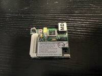
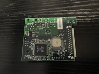
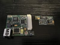
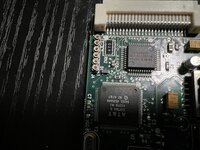
I am selling my stockpile of PowerBook Duos (keeping just two 2300c models) and in the process of readying my others for sale, I stumbled across something that may interest you. Specifically, the PowerPort/Mercury for the PowerBook Duo by Global Village. See attached photos. I have not yet Googled the chips to see if there's any clue to the architecture. Let me know if there's anything I can do to help...
The one interesting note - the RJ-11 port is black - unlike the more common Apple modems' gray. Might be an easy way to determine if anyone else has one of these "rare" Global Village modems either in their collection or for sale elsewhere.
Attachments

My 540 appears to have the PowerPort Mercury installed, if there’s any testing I could do to help LMK!

Bumping this thread with some more info.
Mapped out the pin functions this morning. I'm reasonably confident in the table below with a couple of caveats:
A basic schematic for the digital bits of the factory modem is attached.
I haven't gotten as far with the code that drives the bus. The bus is connected to the power manager IC, so all I'm certain of is that all interaction with the modem must go through the OS Power Manager. The SuperMario sources have been a great source of info about the _PMgrOp trap:
I plan to experiment with using the trap to try to send some commands to a modem. The information above and the RCV144DPL datasheet are probably enough to puzzle out the structure of the relevant commands.
Currently working on reversing bits of the INIT and DRVR resources in the PowerBook Setup control panel for some better end-to-end info.
All told, the simplicity of the interfaces--both software and hardware--seem promising as far as the ability to install arbitrary hardware in the modem port goes. It seems like it might be possible to hang a uC off the bus behind some glue logic that copies what's on the factory board, then access the bus using the power manager commands (e.g. modemWriteReg, modemReadReg, modemWriteData, modemReadFIFOData). That would open up a pretty wide range of possibilities, which is especially exciting given that whatever is installed in that slot has access to the space that would otherwise be occupied by the RJ11 connector.
I'm not sure what the bandwidth of the modem slot is, but I'm guessing that it's fairly low. Can't imagine that a 14.4kpbs modem demanded that much. The overhead of accessing the bus via the SPI-attached power manager also won't help. It'll be interesting to see what's possible!
Mapped out the pin functions this morning. I'm reasonably confident in the table below with a couple of caveats:
- I haven't been able to determine whether or not pins 22, 25, 30, and 38 are connected
- I'm not sure of the functionality of pins 10, 18, 27, and 43. Pin 10 is pulled down and the rest are pulled up to +5V_MODEM
Markdown (GitHub flavored):
Pin | Name          | Type         | Description
----+---------------+--------------+-------------
  1 | `IRQ`         | Output       | Modem interrupt request.
  2 | `/RESET`      | Input        | Modem reset.
  3 | `GND`         | Ground       | Digital ground.
  4 | `A4`          | Input        | Modem address bus.
  5 | `DIR`         | Input        | Data bus direction. When high, the modem drives the data bus; when low, the host drives the data bus.
  6 | `/RBDVR`      | Open coll.   | Relay B Driver from modem card to modem adapter card (DAA) in expansion device - MiniDock or Duo Dock.
  7 | `A3`          | Input        | Modem address bus.
  8 | `+5V_US`      | Power        | Unswitched +5 V. Always on.
  9 | `A2`          | Input        | Modem address bus.
 10 | `PD0`         | Output       | Pulled down via a 4.7k resistor.
 11 | `A1`          | Input        | Modem address bus.
 12 | `/CS`         | Input        | Modem chip select.
 13 | `A0`          | Input        | Modem address bus.
 14 | `MDMSOUND`    | Output       | Phone line monitor. Analog signal.
 15 |               |              |
 16 | `GND`         | Ground       | Digital ground.
 17 | `/WRITE`      | Input        | Modem write strobe.
 18 | `PU0`         | Output       | Pulled up to `+5V_MODEM` via a 100k resistor.
 19 | `/READ`       | Input        | Modem read strobe.
 20 | `/MDMPWR`     | Input        | Power control signal for `+5V_MODEM`. When asserted (low), +5 V appears on the `+5V_MODEM` pins.
 21 | `RAW_10V`     | Power        | Unregulated +10 V. It is on when the CPU is awake (maximum current 25mA).
 22 |               |              |
 23 | `D6`          | Input/Output | Modem data bus.
 24 | `D3`          | Input/Output | Modem data bus.
 25 |               |              |
 26 | `D7`          | Input/Output | Modem data bus.
 27 | `GND`         | Ground       | Digital ground.
 28 | `D2`          | Input/Output | Modem data bus.
 29 | `D4`          | Input/Output | Modem data bus.
 30 |               |              |
 31 | `D5`          | Input/Output | Modem data bus.
 32 | `D1`          | Input/Output | Modem data bus.
 33 | `/RADVR`      | Open coll.   | Relay A driver from the data pump.
 34 | `D0`          | Input/Output | Modem data bus.
 35 | `GND`         | Ground       | Digital ground.
 36 | `/RINGDET`    | Input        | Ring detect signal from an expansion device’s adapter card (DAA).
 37 | `J3`          | Output       | Pulled up to `+5V_MODEM` via a 100k resistor. Connected to ground if J3 is closed.
 38 |               |              |
 39 | `+5V_MODEM`   | Power        | +5 V modem power. On when `/MDMPWR` is asserted.
 40 | `+5V_MODEM`   | Power        | +5 V modem power. On when `/MDMPWR` is asserted.
 41 | `+5V_MODEM`   | Power        | +5 V modem power. On when `/MDMPWR` is asserted.
 42 | `SERVEE`      | Power        | -5 V power. On when CPU is awake.
 43 | `J3`          | Output       | Pulled up to `+5V_MODEM` via a 100k resistor. Connected to ground if J3 is closed.
 44 | `DAA_GND`     | Ground       | Analog ground.
 45 | `DAA_GND`     | Ground       | Analog ground.
 46 | `LINE_T/R`    | Input/Output | Voice-band analog signal to or from an expansion device’s modem adapter card (DAA).
 47 | `KEYSCANX[5]` | Output       | Keyscan line to the Power Manager, for power-on button.
 48 | `DAA_GND`     | Ground       | Analog ground.
 49 | `KEYSCANX[0]` | Output       | Keyscan line to the Power Manager, for power-on button.
 50 | `ON/OFF_OUT`  | Output       | CPU on/off control signal to Power Manager.
A basic schematic for the digital bits of the factory modem is attached.
I haven't gotten as far with the code that drives the bus. The bus is connected to the power manager IC, so all I'm certain of is that all interaction with the modem must go through the OS Power Manager. The SuperMario sources have been a great source of info about the _PMgrOp trap:
- Structure for a _PMgrOp parameter block
- List of commands that are likely related to the modem
- More commands that are likely related to the modem
- List of command sizes for modem-related commands
- Routine for powering on the modem, which calls the power manager to power on and enable the modem and toggles the reset line
I plan to experiment with using the trap to try to send some commands to a modem. The information above and the RCV144DPL datasheet are probably enough to puzzle out the structure of the relevant commands.
Currently working on reversing bits of the INIT and DRVR resources in the PowerBook Setup control panel for some better end-to-end info.
All told, the simplicity of the interfaces--both software and hardware--seem promising as far as the ability to install arbitrary hardware in the modem port goes. It seems like it might be possible to hang a uC off the bus behind some glue logic that copies what's on the factory board, then access the bus using the power manager commands (e.g. modemWriteReg, modemReadReg, modemWriteData, modemReadFIFOData). That would open up a pretty wide range of possibilities, which is especially exciting given that whatever is installed in that slot has access to the space that would otherwise be occupied by the RJ11 connector.
I'm not sure what the bandwidth of the modem slot is, but I'm guessing that it's fairly low. Can't imagine that a 14.4kpbs modem demanded that much. The overhead of accessing the bus via the SPI-attached power manager also won't help. It'll be interesting to see what's possible!
Currently working on reversing bits of the INIT and DRVR resources in the PowerBook Setup control panel for some better end-to-end info.
Of course I haven't gotten anywhere with this because I've been looking in the wrong place. The driver I needed is in the Express Modem control panel (available on the Apple Telecom CD). Hopefully I'll have some time do dig into this next week!
So glad this popped up again, check this out:

 tinkerdifferent.com
"Hearing mention of vestigial implementation on the 230 board for the second serial port just now blew me away! How much higher throughput might that Printer Port(?) connection have than the Modem card interface?
tinkerdifferent.com
"Hearing mention of vestigial implementation on the 230 board for the second serial port just now blew me away! How much higher throughput might that Printer Port(?) connection have than the Modem card interface?
Thinking it might put an entirely new spin what I recall as a Modem WiFi card development in progress?"
Only drawback I can see offhand might be contention with that port when docked? Would serial be faster than modem interface for your project?
Schematics for PowerBook Duo model
Greetings, Those who Tink! In my repair bin, there is a broken 210-Duo. Sometimes, I try to repair it. Very difficult, and my knowledge of the board is too low. On a chance, I was watching a video on youtube of repair a PenLight (tablet machine made from board of Duo). What a surprise...
tinkerdifferent.com
Thinking it might put an entirely new spin what I recall as a Modem WiFi card development in progress?"
Only drawback I can see offhand might be contention with that port when docked? Would serial be faster than modem interface for your project?
Similar threads
- Replies
- 82
- Views
- 18K
- Replies
- 8
- Views
- 3K
- Replies
- 67
- Views
- 16K