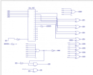
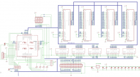
if it were me, I would just shove it all in an XC9536. but eh. Are GALs still manufactured out of curiosity?
Last edited by a moderator:
Yes, Atmel was bought by a company called "Microchip", who are now manufacturing them.if it were me, I would just shove it all in an XC9536. but eh. Are GALs still manufactured out of curiosity?
I checked Aliexpress and they appear to have CMOS in DIP, but of course you're kind of making a bet at what you're going to get. (And be waiting for it for two months.) Personally I'd go with the pair of 74HC138s, that'll take less space than the '154 plus all those resistors unless you go surface mount.I realised I'd miscounted the number of inputs (should be 8 ) after I modified the schematic, so yes a 16V8 will work fine.
As for the 74HC154 they seem to be plentiful from both RS Components and Farnell, but only as SOIC packages.
As for SYS_POWER*, from what I can make out from the schematics it looks like it's there to disable hardware until the system is fully powered (i.e. not in sleep or "shut down"). Admittedly, for the RAM card is should be superfluous, though apparently the SRAM chips run in low-power mode if /CS is forced HIGH.
That adapter alone seems to sell for about $22 quantity one, that's as much as all the active parts plus a decent chunk of a quantity 5 PCB run at an outfit like JLCPCB.The BOM for this design would be a Winslow 9303 adapter, 74xx244, 74HC154, 16V8, a PLCC-44 socket a DIP socket and three resistor networks.

#PACE: Start of PACE I/O Pin Assignments
#NET "iCLK"  LOC = "p1"  ;
NET "A20"  LOC = "p2"  ;
NET "A21"  LOC = "p1"  ;
NET "A22"  LOC = "p44"  ;
NET "A23"  LOC = "p43"  ;
NET "AS"  LOC = "P3" ;
NET "CE1"  LOC = "p39" ;
NET "CE2"  LOC = "p40" ;
NET "CE3"  LOC = "p41" ;
NET "CE4"  LOC = "p42" ;
NET "BANK"  LOC = "p38" ;
NET "OE"  LOC = "p29" ;
NET "WE"  LOC = "p30" ;
NET "BOE"  LOC = "p32" ;
NET "DIR"  LOC = "p31" ;
NET "LED1" LOC = "p19";
NET "LED2" LOC = "p20";
NET "LED3" LOC = "p21";
NET "LED4" LOC = "p22";
NET "DELAYCS"  LOC = "p33";
NET "MUXOUT" LOC = "p5";
NET "NORIN" LOC = "p6";
#NET "DTACK"  LOC = "p34";
No questioning, man.Before you question the design, Keep in mind that this works/worked.
The resistor I was questioning is the one you have on the outputs of your 74HC244 and the inputs of the 154 and the GAL (RN3 on your diagram). That's an HC driving LS; CMOS has a wider voltage swing than LS for a given supply voltage so CMOS outputs should basically always be valid inputs for LS. Not debating that you might need the pull-ups on the outputs of an 'LS154 driving the CS inputs on those old 32K RAM chips.The 154 I can get is the HC version (SIOC package). It's recommended that you use a pull-up between the output of an LS or AC part and an HC one, from what I've read.
It was a "belt and braces" approach and probably not needed but seeing as it's trivial to add to the schematic I thought I'd add it. I could just not fit the resistor array after all and see if it works. If it doesn't that I can easily solder the component on the board, which I couldn't if the holes weren't there.The resistor I was questioning is the one you have on the outputs of your 74HC244 and the inputs of the 154 and the GAL (RN3 on your diagram). That's an HC driving LS; CMOS has a wider voltage swing than LS for a given supply voltage so CMOS outputs should basically always be valid inputs for LS. Not debating that you might need the pull-ups on the outputs of an 'LS154 driving the CS inputs on those old 32K RAM chips.
You'll just be making the CMOS chip work unnecessarily hard when it asserts a "low". Here is a quick rundown. TL;DR, you need the pull-up when going TTL->CMOS, when going CMOS->TTL the main limitation is fanout. Adding a pull-up resistor would just make fanout *worse*, but fanout doesn't matter anyway because you're only driving a single TTL load on each CMOS output of the '244.It was a "belt and braces" approach and probably not needed but seeing as it's trivial to add to the schematic I thought I'd add it. I could just not fit the resistor array after all and see if it works. If it doesn't that I can easily solder the component on the board, which I couldn't if the holes weren't there.
Why not use an HC '244 instead of LS? They're a completely standard part readily available in both DIP and surface mount.It'll be a 74HC154 (there's just not a symbol for that in the KiCad database, but they're pin compatible). I'd still need to pull up the output from the 244 into the 154 as that's TTL -> CMOS (according to what I've read this is required).
GAL16V8  ; memory decoder
MACTHING   ; done

A19 A20 A21 A22 A23 LDS UDS RW AS GND
NC 245DIR MEMCSLOW MEMCSHI 245OE RAMOE RAMWEHI RAMWELO NC VCC

245DIR = RW

/245OE = /RAMOE +
         /RAMWEHI +
         /RAMWELO

/MEMCSLOW = /A19 * A20 * /A21 * /A22 * /A23 * /AS

/MEMCSHI = A19 * A20 * /A21 * /A22 * /A23 * /AS

/RAMOE = /MEMCSLOW * /UDS * RW +
         /MEMCSLOW * /LDS * RW +
         /MEMCSHI * /UDS * RW +
         /MEMCSHI * /LDS * RW

/RAMWEHI = /MEMCSLOW * /RW * /UDS +
           /MEMCSHI * /RW * /UDS

/RAMWELO = /MEMCSLOW * /RW * /LDS +
           /MEMCSHI * /RW * /LDS

DESCRIPTION

; Decoding logic to repair a 1MB Portable memory card
; 245DIR is just a buffered version of R/W direction register on card
; A chart in the Portable (BL) dev note implies this is right
; SYSPOWER isn't used.
; Actual chip addresses need to be decoded by an external multiplexer.You just dont want anything floating that could result in erroneous selections of the ICs when /AS isnt valid for the decode space. Or, accidental bus contention. That too would be bad.I've just checked Farnell, I can get the HCT parts for both the 244 and 154 easily, so that's probably the way to go (rather than mixed LS/HC). That should negate the need for pull-ups at all.
HCT is CMOS process logic (so it uses less power than LS) but it essentially has built-in pull-ups so it can be mixed freely with TTL logic. I've mixed LS and HCT in the boards I built for my Tandy 1000s freely and it works fine. HC, yeah, you have the "pull up" issue.ISTR the HC and HCT identifiers being the determining factor? Have very vague memories of having trouble with one or the other not working with TTL, but that was 30+ years ago so . . . :blink:
So, for sanity's sake, what are the signal levels coming out of the Mac, is it TTL or CMOS? If it's CMOS then I would recommend using HC for everything. (The GAL should be fine with CMOS signal levels.) HCT is *explicitly* for either working as a go-between between TTL and CMOS or to replace TTL with lower power logic. It uses slightly more power and has slightly lower noise resistance than pure HC, if the Portable is CMOS and the RAM chips are CMOS (and the buffers on the card are CMOS) and you can get an HC version of every part there's no reason to use HCT.I've just checked Farnell, I can get the HCT parts for both the 244 and 154 easily, so that's probably the way to go (rather than mixed LS/HC). That should negate the need for pull-ups at all.
