• Hello MLAers! We've re-enabled auto-approval for accounts. If you are still waiting on account approval, please check this thread for more information.

Can a Macintosh use non-contiguous RAM?

I've observed that the Macintosh Plus's memory mapping has many fragmented free segments after the RAM, totaling over 7.8MB. If I were to use two of the larger-looking segments to create 4MB of RAM, creating a mapping structure of 4MB + ROM & IO + 1MB + IO + 3MB, would the additional 1+3MB of memory be usable by applications (System 6)?Or can it be achieved by adding INITs。
In addition, how does SE/30 handle the discontinuity between the front 4MB and the end of the memory?
 
The Plus (and all those using 68000, plus the MMU-less II and the original LC) don't deal with non-contiguous memory very well because they expose the physical address of the hardware directly to the software. In theory, you could use discontinuous area for RAM, but allocating and deallocating memory would be much more complex. For instance, if you have 768 KiB free in each of all three area you described (2.25 MiB total), the system couldn't allocate a 1 MiB block as it requires contiguity.

Anything based on the '030 or '040 (plus the II w/ 68851 MMU) have an onboard MMU, Memory Management Unit. The software uses virtual addresses, that are translated to physical addresses by the MMU. So the MMU (controlled by the OS) takes care of the contiguity, making things much easier. That's why later Macs such as the SE/30 can have "banked" memory of variable sizes (e.g. the Plus requires 1 MiB SIMMs in the first bank if anys is used at all to ensure continuity of addresses). The OS knows which range(s) of physical address really have memory, and when software requires 1 MiB, it will map 1 MiB of contiguous virtual address to 1 MiB of physical memory, one page (can't remember which size System 7 uses, around 2 to 8 KiB probably) at a time. So the physical memory doesn't need to be contiguous.
 
Didn't Connectix RAM Doubler completely rewrite those routines for handling non-contiguous memory? I seem to recall the developers at the time discussing how Apple made all sorts of assumptions in the original code about contiguous memory in how they handled the addressing routines, and Connectix drop-in replaced all that code with a routine that used a more modern memory management model and allowed for non-contiguous addressing even on contiguous memory systems (hence the RAM "doubling").
 
I think a Power Mac 6100 with 64+64+8 MB of RAM has discontiguous physical RAM addresses (in DingusPPC at least). It has a MMU though. I haven't checked if the MMU gets used even if virtual memory is disabled. Should write a debugger routine that dumps the virtual -> physical mappings. The reverse, physical -> virtual, may also be useful but more complicated since multiple virtual addresses can point to the same physical address.
 
I think a Power Mac 6100 with 64+64+8 MB of RAM has discontiguous physical RAM addresses (in DingusPPC at least). It has a MMU though. I haven't checked if the MMU gets used even if virtual memory is disabled. Should write a debugger routine that dumps the virtual -> physical mappings. The reverse, physical -> virtual, may also be useful but more complicated since multiple virtual addresses can point to the same physical address.
That would be very interesting to find out.
 
Is there a meaningful difference between these two?
  • two discontiguous blocks of memory, from A to B and C to D
  • one contiguous block of memory from A to D, with a locked handle from B to C
 
That would be very interesting to find out.
Not so interesting. The CPU can only know a few virtual -> physical translations at one time and DingusPPC can only output those. It's the OS that keeps track of all the translations. An exception handler is used when the CPU tries to access a virtual memory address that it doesn't know about. The exception handler checks the OS's lists of translations to update the CPU's list.

This is from DingusPPC pm6100 with 8+64+64 MB
Code:
6802838C: dingusdbg> regions
--------------
0x00000000..0x007FFFFF (RAM)
0x00800000..0x047FFFFF (RAM,MIRROR) -> 0x10000000..0x13FFFFFF
hole
0x08000000..0x0BFFFFFF (RAM)
hole
0x10000000..0x13FFFFFF (RAM)
--------------
0x40000000..0x403FFFFF (ROM) (BootRomOW)
0x50F00000..0x50F3FFFF (MMIO) (Amic)
0x50F40000..0x50F4FFFF (MMIO) (HMC)
0x5FFFFFFC..0x5FFFFFFF (MMIO) (Nubus-Machine-id)
0xFFC00000..0xFFFFFFFF (ROM,MIRROR) -> 0x40000000..0x403FFFFF

Below is a list of translations that the CPU knows about at a certain point of time (Mac OS 8.6, virtual memory disabled). The list changes as different ranges of code or data are accessed because the CPU can't know all the translations at once.
Code:
6802838C: dingusdbg> translations
00000000..0020FFFF -> 00097000..002A6FFF
00211000..00212FFF -> 002A8000..002A9FFF
00215000..002C6FFF -> 002AC000..0035DFFF
00304000..00306FFF -> 0039B000..0039DFFF
00325000..0032FFFF -> 003BC000..003C6FFF
0036B000..003ADFFF -> 00402000..00444FFF
003AF000..003B1FFF -> 00446000..00448FFF
003CF000..00768FFF -> 00466000..007FFFFF
00769000..00B09FFF -> 10000000..103A0FFF
00B4D000..00B64FFF -> 103E4000..103FBFFF
00BAD000..00BB3FFF -> 10444000..1044AFFF
00C2B000..00C2DFFF -> 104C2000..104C4FFF
04302000..0430FFFF -> 13B99000..13BA6FFF
06488000..06496FFF -> 09D1F000..09D2DFFF
07887000..078BBFFF -> 0B11E000..0B152FFF
078C3000..07995FFF -> 0B15A000..0B22CFFF
07998000..07C4FFFF -> 0B22F000..0B4E6FFF
07CB1000..07CB8FFF -> 0B548000..0B54FFFF
07CC8000..07CDFFFF -> 0B55F000..0B576FFF
07CEA000..07CEAFFF -> 0B581000..0B581FFF
07CF7000..07D05FFF -> 0B58E000..0B59CFFF
07D0B000..07D15FFF -> 0B5A2000..0B5ACFFF
07D24000..07D27FFF -> 0B5BB000..0B5BEFFF
07D34000..07D3CFFF -> 0B5CB000..0B5D3FFF
07D51000..07D51FFF -> 0B5E8000..0B5E8FFF
07D6B000..07D79FFF -> 0B602000..0B610FFF
07DCD000..07DCDFFF -> 0B664000..0B664FFF
07DE2000..07E30FFF -> 0B679000..0B6C7FFF
07E52000..07E5CFFF -> 0B6E9000..0B6F3FFF
07E6B000..07E6BFFF -> 0B702000..0B702FFF
07E7A000..07EA5FFF -> 0B711000..0B73CFFF
07EA9000..07EAAFFF -> 0B740000..0B741FFF
07EAD000..07EADFFF -> 0B744000..0B744FFF
07EB6000..07EC8FFF -> 0B74D000..0B75FFFF
07ECD000..07ECFFFF -> 0B764000..0B766FFF
07F1E000..07F2DFFF -> 0B7B5000..0B7C4FFF
07F30000..07F3AFFF -> 0B7C7000..0B7D1FFF
07F45000..08391FFF -> 0B7DC000..0BC28FFF
08394000..08404FFF -> 0BC2B000..0BC9BFFF
08424000..085C8FFF -> 0BCBB000..0BE5FFFF
085CD000..085E8FFF -> 0BE64000..0BE7FFFF
085E9000..0861AFFF -> 0BEA8000..0BED9FFF
0861C000..0861CFFF -> 0BEDB000..0BEDBFFF
40800000..40BFFFFF -> 40000000..403FFFFF
50F00000..50F01FFF -> 50F00000..50F01FFF
50F04000..50F04FFF -> 50F04000..50F04FFF
50F08000..50F08FFF -> 50F08000..50F08FFF
50F0A000..50F0AFFF -> 50F0A000..50F0AFFF
50F10000..50F11FFF -> 50F10000..50F11FFF
50F14000..50F14FFF -> 50F14000..50F14FFF
50F16000..50F17FFF -> 50F16000..50F17FFF
50F24000..50F24FFF -> 50F24000..50F24FFF
50F26000..50F28FFF -> 50F26000..50F28FFF
50F2A000..50F2AFFF -> 50F2A000..50F2AFFF
50F31000..50F32FFF -> 50F31000..50F32FFF
50F40000..50F40FFF -> 50F40000..50F40FFF
5FFFE000..5FFFEFFF -> 0BEFE000..0BEFEFFF
60B00000..60B96FFF -> 00000000..00096FFF
61000000..61027FFF -> 0BE80000..0BEA7FFF
68000000..680FFFFF -> 40300000..403FFFFF
68FFE000..68FFFFFF -> 0BEFE000..0BEFFFFF


Is there a meaningful difference between these two?
  • two discontiguous blocks of memory, from A to B and C to D
  • one contiguous block of memory from A to D, with a locked handle from B to C
In the former case, the Memory Manager needs a method to know that it cannot use B to C.
In the latter case, the proposed method uses a locked handle (or a pointer).
 
I've observed that the Macintosh Plus's memory mapping has many fragmented free segments after the RAM, totaling over 7.8MB. If I were to use two of the larger-looking segments to create 4MB of RAM, creating a mapping structure of 4MB + ROM & IO + 1MB + IO + 3MB, would the additional 1+3MB of memory be usable by applications (System 6)?Or can it be achieved by adding INITs。<snip>
Throwing my weight of naivety and ignorance into the mix of this.

My understanding is that for some Macs, particularly in the ≥68030 eras, but also going up to the PPC era (e.g. PowerBook 1400), non-contiguous RAM was handled both by custom chips and the MMU. But let's start with the Mac Plus, Mac SE (and presumably the Mac Classic).

They all in fact have hardware to handle non-contiguous RAM. Shock! Horror! Who knew? Well, we all do. If you place 4x 256kB RAM chips in a Mac Plus you get 1MB of RAM, but obviously this can't be using the same addressing as sticking 4x 1MB RAM chips. Instead a crude system using solder jumpers and resistors makes the second bank of 512kB contiguous with the first bank. And this explains why the RAM options are what they are: 1MB, 2MB, 2.5MB 4MB: there's no 1.5MB or 3MB options on a Plus. The DRAM chips of the era multiplexed address lines, so a 256kbit DRAM chip had 9 address lines A0..A8 when the /CAS signal is low which were also used for A9..A17 (/RAS is low). So, the next step up would need to use one more address line, giving A0..A9, which when multiplexed also gives A10..A19 and therefore addresses 1Mbit instead of 256kbit. Hence only two SIMMs were allowed: 256kB and 1MB (though with 64kbit x 4bit chips you can create other options, we'll ignore that).

Hmmm. The 1MB mapping could have been:

An...: A21 A20 A19 A18 A17 A16 A15 A14 A13 A12 A11 A10 A09 A08 A07 A06 A05 A04 A03 A02 A01 A00
Bank0: ..........0 a8. a7. a6. a5. a4. a3. a2. a1. a0. a8. a7. a6. a5. a4. a3. a2. a1. a0
Bank1: ..........1 a8. a7. a6. a5. a4. a3. a2. a1. a0. a8. a7. a6. a5. a4. a3. a2. a1. a0


Where a8.. a0 in bold are the /RAS=0 multiplexed lines And the 4MB mapping could have been:

An..: A21 A20 A19 A18 A17 A16 A15 A14 A13 A12 A11 A10 A09 A08 A07 A06 A05 A04 A03 A02 A01 A00
Bank0:..0 a9. a8. a7. a6. a5. a4. a3. a2. a1. a0. a9. a8. a7. a6. a5. a4. a3. a2. a1. a0
Bank1:..1 a9. a8. a7. a6. a5. a4. a3. a2. a1. a0. a9. a8. a7. a6. a5. a4. a3. a2. a1. a0


But this would have required a9.. a0 to be shifted. Instead it's easier just to map just a9 and a9 to the higher address bits:

An..: A21 A20 A19 A18 A17 A16 A15 A14 A13 A12 A11 A10 A09 A08 A07 A06 A05 A04 A03 A02 A01 A00
Bank0:..0. a9. a9. a8. a7. a6. a5. a4. a3. a2. a1. a0. a8. a7. a6. a5. a4. a3. a2. a1. a0
Bank1:..1. a9. a9. a8. a7. a6. a5. a4. a3. a2. a1. a0. a8. a7. a6. a5. a4. a3. a2. a1. a0


Given the simplicity of the Mac Plus SIMM handling, this is almost certainly how it's done. But the conclusion is the same, RAM in these other Macs is physically, non-contiguous. That's also why you have to put the 256kB DRAMs in bank 1 if you have 2.5MB, because then Bank0 happily generates the addresses for the first 2MB of RAM, and Bank1 only needs to generate up to a8 a8.

Onto later generation Macs. Even though an LCII has a 68030 with an MMU, its Egret chip (I think, edit: wrong it's called V8) handles different sizes of SIMMs, because a similar engineering challenge occurs! Except this time, the bit mangling can be controlled in software. Here, the bottom 4MB of RAM is fixed and must be in the lowest part of physical RAM if no SIMMs are inserted, but if 8MB of RAM is added, the SIMMs must be in the lower part of Physical RAM. Therefore the 4MB of RAM must initially be allocated 8MB of address space anyway and there are a few configuration bits (maybe just 1) which juggles address lines in the same way as for the Mac Plus. The LCII and LC are both limited to 10MB of RAM so the top 2MB of the 4MB of soldered RAM is inaccessible if SIMMs contain 8MB.

The Egret bit juggling is excusable for the LCII, because it basically uses the same logic board as the 68020-based LC which had no MMU. However, 68030 Macs like the IIsi and others had similar, limited options for RAM expansion, and will handle the physical RAM organisation in similar ways: with bit juggling in hardware.

You could also argue that the IIsi needed the hardware bit juggling, because it was released in the System 6 era, which had no support for virtual memory (and couldn't support it, because of the use of high address bits as flags by the OS's memory manager), but in fact similar things happen for the PowerPC Macs like the PowerBook 1400 whose MMU I understand is always active (even if VM is off). Having said this, the MMU in a 68030 could have been used to get around the problem even in the system 6 era by duplicating page tables for every 16MB of address space. Then it doesn't matter what's in the upper 8-bits, it still all points to the same addresses; and it doesn't matter that VM isn't supported because the page tables wouldn't be modified once the OS was booted up. The 68030 supports 32kB page table entries so you need 512 entries for 16MB of RAM and 131072 entries for the entire address space. so, not very practical (perhaps taking up to 2MB of RAM)!

Here, the PB1400 can support multiple odd-ball RAM slots. It has 8MB of soldered RAM + a daughterboard of 4MB or 8MB + 2 User RAM expansions each of which can support up to 32MB. In theory, it could be fitted with 64+16=80MB of RAM, though in fact this is not possible! In a PB1400 there's a physical memory mapping chip which has 32 entries of 4-bits each (16 bytes of IO space, because each byte contains a pair of entries). Each entry represents 2MB of physical address space, sourcing each 2MB from one of up to 8 RAM slots (Logic board, system expansion, then 3x user expansions for both boards). In theory, and there's some discussion about this on the 68KMLA, software could reprogram these on the fly to bank-switch in the other 16MB of RAM that's not usually available. This would almost certainly lead to a crash!

Is there a meaningful difference between these two?
  • two discontiguous blocks of memory, from A to B and C to D
  • one contiguous block of memory from A to D, with a locked handle from B to C
There has been some discussion about this for the Mac Plus and other 4MB Macs. The major reason why you need a gap is because the Mac Plus (and SE and Classic) have ROM sitting at 4MB, even though its only 128kB, so you could (in theory) add nearly 4MB of RAM on top until you hit I/O.

I made some progress on it. I don't think it's practical to create a locked handle to exclude the ROM gap, because by the time the OS has booted, The OS has already limited RAM to below the ROM. What I have proved is that you can run an app which launches another application with a specific memory allocation that takes the bottom of it's memory allocation to just above the gap you want to create; then launch a third application whose size forces the bottom of it's memory to just below the gap you want (thus that app covers the gap), then quit all the other apps, leaving that app occupying a hole in the Mac's memory.

Then what you'd do is implement that in a early INIT: adjust System RAM so that it's 8MB not 4MB; create a fake application that covers the ROM area; then the INIT quits, leaving a gap for the system to work around. You wouldn't be able to allocate 6MB of contiguous space in an app (obviously), but you could have 2x applications using 3MB each or you could have an app which used its own 3MB of RAM and allocated system RAM (dangerous) for access to up to 3MB more, or so, of RAM.

Check out AppGap:
 
Last edited:
They all in fact have hardware to handle non-contiguous RAM
Pretty sure it's not the case for the 68k based systems. Non-contiguous addresses visible from software is a massive pain (as all those who tried to increase the amount of memory in those old systems quickly find out). Much easier to make memory contiguous in hardware.

If you place 4x 256kB RAM chips in a Mac Plus you get 1MB of RAM, but obviously this can't be using the same addressing as sticking 4x 1MB RAM chips. Instead a crude system using solder jumpers and resistors makes the second bank of 512kB contiguous with the first bank
... so the memory *is* contiguously addressed then :-) The hardware modification needed is indeed just to make sure the second bank is mapped at the appropriate address to ensure continuity with the first one.

You could also argue that the IIsi needed the hardware bit juggling, because it was released in the System 6 era, which had no support for virtual memory
There's no bit juggling in the IIsi, it is just using the MMU to remap the memory inside the ROM (as is done on every machine with a MMU). Both banks are physically on 64 MiB boundaries, the ROM find out the actual installed sizes and build a table for the rest of the ROM and the OS (including handling the area reserved for the onboard framebuffer), and then the MMU maps a contiguous area of virtual addresses to the physical addresses. Look for functions MakePhysicalMap, InitMMU, FindInfo, ... in the ROM source code. Later memory controllers are programmable and can map the banks in a more versatile way, but ultimately the MMU is always used (it's there, it's convenient, might as well!).
The IIsiFPGA ROM patch adds a third entry to the bank table, then patch the ROM code to handle the extra entry properly. While the original banks are at 0x00000000 and 0x04000000, the IIsiFPGA bank is at 0x20000000 - it has to be aligned on a power-of-2 boundary at least as big as the bank size and it can be up to 240 MiB. The MMU hides all that from the user.

MMU are awesome. My favorite is the design from the Sun-2 and Sun-3, which could do zero-cycle translation for the '010 / '020 thanks to a clever meshing with the behavior of the memory controller. Unfortunately the trick they use doesn't work with 8-bits SIMM larger than 4 MiB (on the Sun-3), or 32-bits SIMM, which makes adapting Sun-3 to newer SIMM a pain (Sun-2 can't use more than 7 MiB anyway).
 
Is there a meaningful difference between these two?
  • two discontiguous blocks of memory, from A to B and C to D
  • one contiguous block of memory from A to D, with a locked handle from B to C
That's the perfect question to ask.

There are basically two functions that are interesting here. One for requesting the amount of free ram and one for allocating some.

Although it seems so, most systems don't allow you to request the total free ram. Instead they allow you to request the size of the biggest contiguous chunk which in turn is the max amount you can allocate in one request.

So I'd say it's quite straight forward to make some additional ram available to the plus. You would not be able to allocate one huge block. But once e.g. the primary 4MB area has been used some additional area in another spot may become the biggest one and be used to fulfill further allocation requests.
 
Pretty sure it's not the case for the 68k based systems.
Pretty sure that the V8 memory controller on the LC and LCII make sure non-contiguous 4MB (or 2MB on the LC) and SIMM DRAM appear contiguous, because the LC has a 68020. It can’t use an MMU to do that. Also pretty sure the LCII ROM is almost exactly the same as the LC ROM and therefore doesn’t use the MMU to make ram contiguous if VM is off.
Non-contiguous addresses visible from software is a massive pain <snip> Much easier to make memory contiguous in hardware.
Agreed.
... so the memory *is* contiguously addressed then :)
I guess what I meant is that at some hardware level, memory on a number of Macs going back to pre-‘030 Macs is discontiguous and so therefore it’s been an ongoing design issue to solve with increasing sophistication. I’m presenting a (weak) argument that the Mac Plus & SE have a super-primitive memory controller that involves component mods; the LC and LCII a slightly better one.


There's no bit juggling in the IIsi, it is just using the MMU to remap the memory inside the ROM (as is done on every machine with a MMU). Both banks are physically on 64 MiB boundaries, the ROM find out the actual installed sizes and build a table for the rest of the ROM and the OS (including handling the area reserved for the onboard framebuffer), and then the MMU maps a contiguous area of virtual addresses to the physical addresses. Look for functions MakePhysicalMap, InitMMU, FindInfo, ... in the ROM source code. Later memory controllers are programmable and can map the banks in a more versatile way, but ultimately the MMU is always used (it's there, it's convenient, might as well!).
The IIsiFPGA ROM patch adds a third entry to the bank table, then patch the ROM code to handle the extra entry properly. While the original banks are at 0x00000000 and 0x04000000, the IIsiFPGA bank is at 0x20000000 - it has to be aligned on a power-of-2 boundary at least as big as the bank size and it can be up to 240 MiB. The MMU hides all that from the user.

I’m certainly right about the PB1400. I didn’t know the IIsi had the MMU switched on even in System 6. Still, I’m puzzled, how did they get around the 24-bit addressing? Was MODE32 always part of the IIsi OS?

64MB banks are massive for 1990! I thought the IIsi could only support, like 17MB or so, but I can see from EveryMac that it supports 65MB, which would be 1MB (mobo)+2x32MB.

So if the MMU is always used to remap physical RAM on an ‘030 machine, does this mean an LCII could support more than 10MB via PDS and a suitable INIT or PDS ROM?

Do you have a link to the IIsi ROM listing? Or is it found via the patch you linked to?


MMU are awesome. My favorite is the design from the Sun-2 and Sun-3, which could do zero-cycle translation <snip>
Yes they are. Except for segmented MMUs which are a total pain. From time to time I’ve explored VM algorithms for segmented systems that aren’t depressingly inefficient and also fairly feasible for hobby developers.

The 80286 is a prime target because few 286 OS’s actually used the MMU to provide proper VM, instead DOS Extenders allowed apps to run within physical memory limits up to system RAM, and could swap out other apps. AFAIK you couldn’t run a 4MB app on a Windows 3.1 PC in ‘286 mode. Having said that, perhaps OS/2 1.x and Xenix could manage it.

My approach would be to link code into 4kB segment chunks and similarly aim to chunk data allocation into 4kB chunks (small memory allocations could share segments). That way it could be managed similarly to a paged MMU and the 8k or so of LDT segments available could support up to 32MB apps+data.

I also looked the Interdata 7/32 (or 8/32), which was the second computer to support Unix (via the work done at a ln Australian uni). Those computers have a 1MB physical and virtual address space but only 16 segments so it’s not practical to waste segments to mimic a paged MMU. Aligning segment sizes to multiples of 4kB and only swapping in enough of any segment to meet needs, would help I think.
 
I think I’ve figured out how an MMU can map discontiguous RAM at eg 64MB offsets and then run 24-bit mode System 6.

It’s not too trivial, but this is how I’d do it. You set up 16MB worth of page tables (you only need 16MB/32kB=512 entries). To create the page table entries that map the rest of address space, you just make use of the multi-level PTEs, the rest of the top level entries point to the same Page Table as the first one.

It doesn’t matter then if you run system 6 which can only cope with 16MB, System 6 only sees the virtual addresses even though it’s running in Supervisor mode (did ‘030+ Macs still run in Supervisor mode? I think it would still apply).
 
Pretty sure that the V8 memory controller on the LC and LCII make sure non-contiguous 4MB (or 2MB on the LC) and SIMM DRAM appear contiguous, because the LC has a 68020. It can’t use an MMU to do that. Also pretty sure the LCII ROM is almost exactly the same as the LC ROM and therefore doesn’t use the MMU to make ram contiguous if VM is off.

First, my bad, should have written "68000" in the paragraph you answer to, not "68k". Though my point (you need contiguous memory at the hardware level) also apply to fully MMU-less 68020 (from the '030 onward, the MMU is used).

As for the LC and LCII, the easiest way it to quote Apple's comments in the source:
; Roll-in LC II changes. Add MMU templates for LC II,
; modify InitMMU routine so that the exception vector table
; contains logical instead of physical addresses, modify @VISA
; routine to load up A0 and A1 with MMU templates, and modified
; routine doPhysROM to build the ROM entries according to the way
; the physical templates are defined if the ROM physical size is
; not 256mb.
(...)
; .(VISA has MMU similar to HMMU) <12><T22>
The LCII has and use the MMU in the '030, and apparently the LC has minimalist support as well (HMMU is the very limited MMU that Apple was putting in Mac II, that can be replaced by a MC68851 to get a full-blown MMU with protection and everything).

I guess what I meant is that at some hardware level, memory on a number of Macs going back to pre-‘030 Macs is discontiguous
On all 68000 Mac (which have no MMU), contiguous address from the CPU are always mapped to contiguous physical memory.
On all 68020 and later, there is aither a full-blown MMU or a HMMU, and it's used to remap the memory. The HMMU is very minimalistic and can only do this basic remapping as I understand it (MMu can do proection, paging, ...).
I was wrong about the MMU-less II and LC in my original answer; it appears the HMMU from the II is also in the LC and is used to do the remapping.

I’m certainly right about the PB1400
The PB1400 is PPC, they all have onboard MMU so have no issue with discontinuous memory either.

64MB banks are massive for 1990! I thought the IIsi could only support, like 17MB or so, but I can see from EveryMac that it supports 65MB, which would be 1MB (mobo)+2x32MB.
Maximum memory and bank size is just how many address lines are connected for row/column; with a MMU you don't have to worry too much and can connect as many as the physical device (SIMM) is specified for. Then the MMU can do the magic for you.
Support in those days meant "this will work, we have verified it". Larger SIMMs weren't always already available, so Apple commonly didn't claim support for them in systems, even if the hardware (and often the ROM) work with them.

So if the MMU is always used to remap physical RAM on an ‘030 machine, does this mean an LCII could support more than 10MB via PDS and a suitable INIT or PDS ROM?
Yes and no... The LCIII definitely can, as its PDS is full-blown and appart for a different patch to the ROM it should work like the IIsiFGA does on the IIsi.
The LCII PDS is the same as the LC IIRC, and will miss some address lines. i don't think it would work, but I haven't checked thoroughly. If not it's a purely electrical/mechanical limitation, adding other memory bank(s) to the MC68030 is only a physical memory map (where to put it) and software (making the ROM/OS aware) issue.

Do you have a link to the IIsi ROM listing? Or is it found via the patch you linked to?
Original source code is floating around such as as "mac-rom" and the supermario source.
For the IIsi, I analyzed the ROM with Ghidra to figure out what I needed to do.
Beware the source are not necessarily complete, Apple was removing some of the old code for newer use of the ROM :-(

Yes they are. Except for segmented MMUs which are a total pain
Technically the Sun-1/2/3 MMU are "segmented"... Whomever wrote the NetBSD support code isn't fond of them either. I can't disagree, but in the historical context they made sense...

I also looked the Interdata 7/32 (or 8/32), which was the second computer to support Unix (via the work done at a ln Australian uni). Those computers have a 1MB physical and virtual address space but only 16 segments so it’s not practical to waste segments to mimic a paged MMU. Aligning segment sizes to multiples of 4kB and only swapping in enough of any segment to meet needs, would help I think.
It was very much an ongoing R&D area in those days. The Sun MMU has a hadware context register (so you can have mappings for up to 8 different context in the segment map). This and some of the virtual bits are used to index the segment map to produce a segment number; this segment number and another 4 virtual bits are used to index the physical map to produce the page number - each segment is 16 consecutive pages in virtual space (which can be discontinous in physical memory). It's not ideal in terms of versatility, but it can map up to 32 MiB of memory at any one time. On systems shipping with 4 or 8 MiB by default it's plenty.

Page indexing bits (straight from the CPU) are used for row addressing, while page number are used for column, and on e.g. the Sun 3/60 the latency of the MMU is fully masked and adds zero wait state. The '851 added 4 cycles (and was late and expensive), so Sun carried the Sun-2 MMU design ('cause the '451 sucked as well and IIRC the SUN predated the '451) slightly expanded to the Sun-3 for performance reason. And probably it made porting SunOS easier as well.
 
First, my bad, should have written "68000" in the paragraph you answer to, not "68k". Though my point (you need contiguous memory at the hardware level)<snip>
OK - compromise: on a 68000, you need contiguous memory at the CPU level :) !
As for the LC and LCII, the easiest way it to quote Apple's comments in the source: .. IIsi, I analyzed the ROM with Ghidra..
The LCII <snip> MMU <snip> LC <snip> HMMU
Interesting. I suppose VISA means the "V8" memory controller chip, which contains a subset of the HMMU? I searched for the ROM listing, haven't found it yet.
<snip> The HMMU is very minimalistic.. <snip> I was wrong about the MMU-less II
Yes, that's what I'm talking about. I think that it's fair to say at least one memory controller; whether on-chip or off-chip; minimal or complete will be used.
The PB1400 is PPC, they all have onboard MMU so have no issue with discontinuous memory either.
And yet, and yet... as detailed in my comment here, the PB1400 (and I think the PB5300) uses what's called a PBX chip to perform physical to physical address mapping before it gets to the CPU's MMU.

index.php


PBX contains 16 bytes x 2 x 4-bit entries for 32 x 2MB (=> 64MB) physical RAM slot and each entry is the bank number of the RAM module. Each bank can be up to 16MB. There's bank 0 is for Motherboard RAM (8MB) bank 1 for the Factory RAM card (usually 4MB or 8MB, but I think 12MB or 16MB is theoretically possible). Then banks 2..4 and 5..7 are for the user expansion RAM expansion slots. e.g. a 64MB fully expanded PB1400 might have PBX set up as: User2 Bank0

Physical Addr0MB2MB4MB6MB8MB10MB12MB14MB
0MBMotherboardMotherboardMotherboardMotherboardFactoryFactoryFactoryFactory
16MBUser1 Bank0User1 Bank0User1 Bank0User1 Bank0User1 Bank0User1 Bank0User1 Bank0User1 Bank0
32MBUser1 Bank1User1 Bank1User1 Bank1User1 Bank1User1 Bank1User1 Bank1User1 Bank1User1 Bank1
48MBUser2 Bank0User2 Bank0User2 Bank0User2 Bank0User2 Bank0User2 Bank0User2 Bank0User2 Bank0

<snip> The LCII PDS is the same as the LC IIRC, and will miss some address lines.<snip>
Fair enoughg.
Technically the Sun-1/2/3 MMU are "segmented"... <snip> It was very much an ongoing R&D area in those days. <Summary: 8-different contexts via Sun MMU reg + virtual bits index segment map+4 virtual bits index phys map => page number>
Yes, I think I read about it a while back, possibly when this last cropped up.

<snip> Sun 3/60 the latency of the MMU is fully masked <snip> the '451 sucked <snip>
Yes.

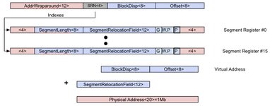
So, to resume about segmentation. True, segmented MMUs were an ongoing topic in the late 60s through early 70s, e.g. MULTICS, pdp-11 have segmentation concepts built-in (e.g. the pdp-11 has 8 regions in its VM space, controlled by segment registers which access a variable length page up to 8kB each on 32b boundaries within a 256kB and later 4MB physical address range).

What really screwed up the 80286 implementation was the byte granularity for the translation addresses and segment lengths, which forces lots of physical memory fragmentation and/or shuffling segments around in physical memory whenever segments need to expand. Whereas, when segments (or pages) are allocated on a fairly coarse granularity (256b, 4kB like a PMMU) it actually gets easier. At the time, Intel was trying to copy MULTICS, but failed to properly understand that its GE implementation of virtual memory used both segmentation and a form of page addressing. Even earlier computers like the pdp-10 (and pdp-9) which themselves used a terribly crude segmentation scheme still had coarse granularity from memory.

That's why the Sun segmented MMU (though crude) was better - segmentation still sat on top of pages.

The Interdata 7/36 had a much more sensible page size, and in some senses was trying to emulate pdp-11 style VM (though with 16 segments). Here the big mistake, IMHO was to fail to sufficiently abstract segments and so segments will tend to expand to 64kB before the next segment is used and so the VM mapping would be full of 64kB segments, with huge swapping penalties.

Interdata736.jpg
Having said that, it does look a lot like your description of the Sun MMU. And, I think there may be (horrible) ways to mitigate it, namely, by distributing allocated memory amongst as many segments as possible before expanding segments. Even then it's nasty, because, for example, it's conventional to allocate code to consecutive addresses, so a 64kB application would occupy a whole 64kB of segment 0 and then the VM manager has the same problem: it must swap out 64kB of code at a time. And if you didn't do that, by distributing code allocation, you'd rapidly use up segments which you'd probably want to use for data.

So... what's a better solution? Well maybe the 68K Macintosh handle-based memory manager might even be helpful. Code or text segments could then prefer to be small. Then they could be distributed amongst segments alongside data allocations and moved around to better optimise swapping. The big difference would be that the memory manager wouldn't want to compact memory blocks consecutively, but compact blocks across segments as evenly as possible. The upsides are that it would improve swapping performance and you could have applications larger than the physical and virtual memory space (because a Mac-style jump table can do that); the downside is the complexity of additional indirect access, because software is doing what hardware should be doing and reliability, because code and data gets intermixed and you can't allow a return to a code segment that's been unloaded.
 
Technically the Sun-1/2/3 MMU are "segmented"... Whomever wrote the NetBSD support code isn't fond of them either. I can't disagree, but in the historical context they made sense...
I just wanted to read up on that again.


1762122406361.png
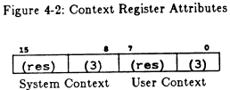
In modern terms, a Context is like the ASID bits on a MIPS R3000: it allows multiple page tables to be present on the system and to switch between them by changing the context itself. In modern terminology the Sun 2 MMU has 8 process tables of 512 entries each, where each entry is selected from bits <23:15> of the Virtual address for the current supervisor or user process. The contents of entry is an 8-bit value, which points to 256 x 16 page tables (called Page Maps); where the specific entry is taken from bits <14:11> of the VA and each entry in each table is:

1762122782917.png
Thus any entry can point to any physical page in the physical address space. Finally, bits <10:1> of the VA access the 16-bit word within the page. Thus, the Sun 2 MMU is a multi-level page-table MMU:

PA=(PageMap[ (SegMap[(Context[FC==5 || FC==6]<<9)|(VA>>15)]<<4)|((VA>>11)&15)]<<11)|(VA&0x7ff);

There's no bounds field in the MMU and every virtual page within a segment can be freely mapped to a physical page anywhere in RAM (or ROM, or IO space I suppose). The full, physical address range is 20+11 = 31 bits! The clever thing is to use the FC pins to increase the VA to 24 bits (32MB, as you said) rather than 16MB on a normal 68000 or 68010.
 
Last edited:
In modern terms, a Context is like the ASID bits on a MIPS R3000: it allows multiple page tables to be present on the system and to switch between them by changing the context itself.
Which is neat. But Sun must have realized it was a bit overkill in the Sun-2 implementation which you look at; in the Sun-3, the two fields (Supervisor and User) were removed to have only one for both.

They also simplified the permission bit a lot, going from 6 to 3 (if you count valid). They also added statistic bits, which are a PITA because they need updating on every access so must have their own write signal potentially (still need to try if I can just rewrite all the non-address bits on all access to simplify, but now that I have splitted them like on real HW...)

You can find my re implementation of those MMUs here and here.

The clever thing is to use the FC pins to increase the VA to 24 bits (32MB, as you said) rather than 16MB on a normal 68000 or 68010.
You misread that. The Supervisor bit (FC[2] indicates a Supervisor access in the predefined spaces), sort-of except for FC==7 which is an interrupt cycle on the '010/CPU cycle on the '020 and FC==4 is reserved) is used to select context depending on whether the access is Supervisor or User. That's on the Sun-2 only; on both architecture, it's also used to check vs. the Supervisor permission(s).

Contexts are limited to 16 MiB virtual space each. Physical space could have been expanded to 31 bits per the spec, but the specifications for type 1 (Multibus like the 2/120 whose manual you linked) and type 2 (VME) Sun-2 both limit physical address space to 23 bits. You get up to 7 MiB of memory and 1 MiB of I/O. It's not a lot, but NetBSD still fit somehow!

EDIT: to clarify, the context register needs to be reloaded with a supervisor-only 'movsb [with FC=3]', so there's no way for a user process to exploit more than one context at once (they can't access the supervisor context on a Sun-2, either). The OS kernel can, in theory, have access to all hardware context by reloading the ctx register.

The Sun-3 (the one for which I mentioned the 32 MiB) expands this, but in practice machines like the 3/60 don't bother implementing all the physical bits (19 bits of page number, 8192 bytes each) of the 4 GiB address space. Not putting the extra SRAM for the upper 3 bits of physical address saves money and board area, I guess. I've actually discussed with some interested parties expanding a 3/60 to a larger MMU, as modern SRAM are much cheaper and much larger and the Sun MMU model can be easily expanded in a backward-compatible way (hence the WiP FPGA recreation as a test bed).

Edit: sorry, this seems to be getting off-topic from the original subject...
 
Last edited:
<user/supervisor contexts> overkill <snip> Sun-3 <snip> only one for both <snip> simplified the permission <snip> 3 <snip> statistic bits, which are a PITA <snip> my re implementation of those MMUs here and here.
Interesting.
You misread that. <snip>
True, I was thinking of how separate instruction/data contexts would have provided a sort-of 32MB address range (like the pdp-11).
<snip> Physical space could have been expanded to 31 bits <snip> You get up to 7 MiB of memory and 1 MiB of I/O. It's not a lot, but NetBSD still fit somehow!
I knew it wasn't actually 31-bits, 1GB in the early 80s would have been even greater overkill. The Sun 3/60s we had access to at UEA, I think were just 16MHz (or 20MHz) '020 Workstations with just 4MB (pretty sure, not 16MB). But 4MB seemed more than ample to my mind for that era. They ran VLSI design in 4MB on suntools (or sunview, but certainly not Solaris).
<snip> context register needs to be reloaded with a supervisor-only 'movsb [with FC=3]'
I assumed it was protected.
<snip> I've actually discussed with some interested parties expanding a 3/60 to a larger MMU <snip>
A better Sun 3/60 than Sun's 3/60 :-) !
Edit: sorry, this seems to be getting off-topic from the original subject...
So, in that tradition, I'll continue off-topic briefly, before steering back.

Lots of computer designs needed to deal with non-contiguous banks of RAM in the era of SIMMs or expansion cards that supported multiple DRAM sizes. A memory controller of some kind needs to map these banks into a contiguous logical memory space. A 68000 (and 68020) lack an MMU, so glue logic had to do that, but an '030+ Mac (or '020 with an MC68851 MMU) can use its MMU and the ROMs did that too, even in 24-bit addressing mode (it turns out to be fairly easy to mask out the top 8 bits using the page table hierarchy).

MMUs have a convoluted history and were a hot topic in the 1960s and 1970s, which was a period just before Macs came out (from the perspective of 2025). Segmented base & bounds MMUs (as on the 80286) turned out to be a messy dead-end, but the lack of standard MMU conventions led early workstation companies like Sun to implement their own Page-based MMU, within which they used "segment" terminology, though it's not a base & bounds design (whew!).

The scrappy evolution of microcomputer OS's delayed the proper use of MMUs for about a decade, until the early/mid 1990s. This wasn't helped by ironically overly complex MMU designs (eg the '040 MMU is simpler than the '030 MMU which is simpler than the MC68851, practical '386 VMMs ignored segmentation). If it was me, I'd have started with a super-simple page based MMU that only worked for user-code. This doesn't mean simple MMUs were never designed: the ARM2's MEMC controller was very simple (a fixed 128 entry inverted table whose page size was determined by the size of physical RAM, up to 4MB). Even then RISC-OS didn't do proper VM.

Back To The Topic

Summary: periodically, people raise the question of adding more than 4MB to a 68000 Mac and the same responses pop up: RAM could be added after the ROM addresses (and perhaps in a few other holes), but it would be non-contiguous. Enabling early System versions to use it is still a problem to solve (though some progress has been made). In either case, an app wouldn't be able to have a partition encompassing non-contiguous RAM. The simplicity (or nearly entirely non-existence) of early microcomputer hardware memory management (as discussed) is a corollary of these early Macs' memory management from a software view.
 
True, I was thinking of how separate instruction/data contexts would have provided a sort-of 32MB address range (like the pdp-11).
Not in "normal" use, but sort-of in "boot" mode. When the PROM first starts running on a Sun-2/3, a bit in a hardware register is set to "boot mode". While this bit is set, FC=6 accesses (Supervisor Program) are directed to the PROM itself, rather than memory. The Sun-2/3 can't bypass the MMU, so they need such a bypass to be able to configure the MMU (which, alongside other piece of hardware, is accessed with FC=3). Once all the hardware has been set up and the PROM mapped by the MMI, "boot mode" is disabled for the console monitor and later OS.

Use of FC for anything other than identifying interrupt ('010) and CPU ('020/'030) cycles were uncommon - the Macs sure didn't bother. I ended up fixing/reporting a few minor bugs in the Suska 68K30L (the soft-core powering my Sun-3/F in FPGA) related to FC, presumably because no other hardware really tested that behavior.

The Sun 3/60s we had access to at UEA, I think were just 16MHz (or 20MHz) '020 Workstations with just 4MB (pretty sure, not 16MB). But 4MB seemed more than ample to my mind for that era. They ran VLSI design in 4MB on suntools (or sunview, but certainly not Solaris).
Sun 3/60 would ship with 4 or 8 MiB, up to a maximum of 24 MiB. They have 6 banks of 4 SIMMs, and can only take 1 MiB SIMM. They said 20 MHz, but it's really 19.6608 MHz :-) Important for a redesign because it's 4*4.9152 MHz, and the 4.9152 MHz clock is fed to the serial port chips (8530) to be divided by 512 to produce the 9600 bauds signals...

Incidentally (and very slightly on-topic), the memory banks are using constiguous addressing and are expected to be filled "in order" (with interleaving making things a bit annoying to understand). It could work discontinuous in theory as there is a MMU, but the PROM doesn't bother and just fill the MMU with 1:1 mapping and then walk from 0 to the first timeout bus error to fugre out the size of the memory. Simpe but effective.

A better Sun 3/60 than Sun's 3/60 :) !
Well, for now the FPGA version is worse - no async SRAM in a FPGA, so you need a couple of cycles to go through the SMAP and PMAP. And the clock is not faster for now to make the serial ports happy - and because the 68K30L is a huge beast that doesn't clock very fast anyway. And it has no meaningful I/O (ethernet or SCSI), so you can't do much with it. Apart from that it's great :)

Tried recreating the Ethernets (82586 for Sun-2 and early Sun-3, Am7990 for later Sun-3 and also used in many Sun-4), but while AI tools pretend to be able to do it (they will happily write you verilog straight from the datasheet!), even the simplest bits (that I can actually understand) contain bugs :-( Even something simpler like the TOD clock I ended up rewrinting most of the code to make it synthesized correctly...

The scrappy evolution of microcomputer OS's delayed the proper use of MMUs for about a decade, until the early/mid 1990s.
... for home computers. Anything running a flavor of Unix had a proper MMU properly used from the 80s (I do count Sun's among those).

Unless you definition of "proper use of MMUs" require a hardware page walker, in which case I'm not even sure when that showed up first. It was there in Sparc V8 hardware, but I'm not sure if some V7 variant had one (there's different MMUs in different generations of sun4) - shame on me! I need to look that up.
 
. It was there in Sparc V8 hardware, but I'm not sure if some V7 variant had one (there's different MMUs in different generations of sun4) - shame on me! I need to look that up.
It's a feature of the reference MMU defined with SPARC V8; V7 systems (sun4, sun4c) only use variants of the Sun-style MMU (inherited from the suN1, sun2 and sun3), while V8 systems (sun4m, sun4d) use a more conventional MMU and a hardware page walker. And for completeness, the offshoots: sun3x uses the MC68030 MMU, while "RoadRunner" (the Sun 386i workstation) uses the 80386 MMU.
 
Back
Top