Generally I go with "Computer Architecture, A Quantitive Approach". Their central premise is that it's the whole system that matters, so there are always trade-offs between clock speeds, pipeline depth, CPI (or IPC), Cache, Bus width, transistor counts; temperature envelopes and whatever other parameters can affect the system.
Still the best reference. The thing to understand - and that is far from obvious - is that pipelining is expensive in area. Whenever a pipeline stage is cut in half to boost frequency, it means that all signals have to be registered in the middle (the value of the signal has to be captured into storage). That is costly. In fact, I only realized how costly it could be when I tried to change the depth of pipelining for FP operators using
FloPoCo for my '883. I didn't need a lot of frequency (being synchronous to a 20 MHz '030), and it will always be better than the '881/'882, so I was ready to use whatever depth of pipelining would use the least amount of area and would be easy to place and route by Vivado. Turns out, making the operators (mul, add, but div and sqrt are the big one that won't fit together) more pipelined took more area, and by a wider margin than I expected. Unlike back then, we now have access with thing like FPGA and FloPoCo to the tools to see and learn about such things for ourselves, which is awesome IMHO.
I think the 21064 did well with about 1.68M transistors.
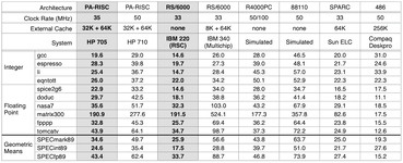
The 21064[A] were pretty good CPUs, but were expensive at the time, so the performance/$ wasn't a game-changer. The '66[A] were a bit too downgraded (the comparison to the SuperSPARC above tells it eloquantly).
In fact, most Alpha CPU were pretty good or great CPU - but the performance gap was much lower than the frequency suggested, and when the price was taken into account, the value proposition wasn't all that great. Sun workstations might not have been the fastest (though that reputation came partly from the low frequency of the SuperSPARC, which had double-pumped parts that were acting on both the positive and negative edge of the clock, so effectively running at twice the clock speed, once you look at CPU 92 or CPU 95 they were in the right ballpark), but Sun had invested heavily in the software side and so it was a better choice for many people.
So, in some ways it's like a PPC603. From your ods table it scored 63.7 from a 66MHz clock (not bad); while a 125MHz A21064 scores 68.4 with 256kB L2 (while a 100MHz A21064 can get 74.6, 150MHz gets up to 81).
I think that illustrates your point quite well.
Good choice of comparison for this forum. I don't think many of us thinks of a 66 MHz 603 as "fast", yet many people would think of an Alpha as "fast". It's all relative to what was available at the time. In fairness to Alpha, the 603 was a later design, so may not be an entirely apple-to-apple comparison. But then it was also a lot cheaper and less power-hungry.
The best 601 in the table is a Bull system with a 75 MHz 601 and 1 MiB of external cache, scoring 93.8. That puts him in the ballpark of a 200 MHz 21066A (the ~230 MHz ones score ~100). Not bad, and all tested in '95. Frequency is not all there is to performance - a 55 MHz POWER2 gets 97.6!
The 90s were all about brainiac (POWER and other low-frequency, high IPC designs) vs. speed demon (high frequency, lower IPC designs). Alpha and POWER were the poster children, and then Intel decided to play the frequency game with AMD in the P3 era and introduced the last great speed demon with the Pentium 4. They won the game, sort of... And yet somehow I still think of Tejas (the cancelled next-P4) and EV8 (the cancelled 21464) as missed opportunities. When Intel presented their P4 roadmap to my research team back somewhere in '99 or '00 (or 01'? can't remember), the (un?)official goal for the P4 family was to reach 10 GHz soon-ish

That was a fun era to do comp.arch .
I tend to think that in the same way that it's possible to improve the performance of software by ploughing more people into the problem, you can also increase the performance of hardware by doing the same thing.
More people well managed can help software; for hardware you soon reach the limitations of the process. Intel used the extra people to hold out on "full-custom" designs longer than everyone else, but I expect they've been doing standard cells for a long time now. Those extra people probably helped a bit, but I wouldn't date quantify by how much.
For those who don't do silicon design for a living, "standard cells" means the foundry (TSMC, Samsung, ...) supplies a bunch of standardized "basic building blocks" (NAND gate with 2/3/4/5/... inputs, single-bit register, ... there's hundreds of them usually, shipped with the
Process Development Kit) that go on a "grid" that supplies the power and ground lines. The place-and-route software uses those building blocks to implement the design synthesized from the RTL (verilog, VHDL, ...). It's the standard way of doing things now (and for a while), and there's usually
a choice of libraries of cells with different criteria (speed vs. size vs. consumption vs. ...).
"full custom" means everything is customized - down to the transistor placement and power lines. It's incredibly complex and time-consuming, and in the 90's the designs gurus capable of optimizing that aspect were highly sought after.
"full-custom" was the only way in the early days (60s, 70s). Then came the gate array chips (80s) - with the transistor pre-placed, and only the metal layers were customized by customer like Apple (most of the custom chips from Apple were gate-array designs). The manufacturer would supply a place-and-route software, and
a library of basic transistor configuration or "cell" [1] (same name, same description!) that would be used by the customer to translate from the schematics to the software. That idea slowly spread to regular ASIC and became the "standard cells" approach.
[1] That would be the document to look at to reverse-engineer many Apple ASIC of the 80s from a die shot, in case anyone want to tackle that


