Gossamer's Tale
The quest for onboard cache
The quest for onboard cache
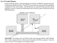
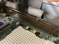
I have been looking around for hints on how to install the 2nd-level cache slot on the beige G3. There is unpopulated component, most likely a socket, that is labeled cache and is connected to the Grackle bridge. The pinout is in the schematics.
Sadly, i could not find a source for the cache slot component. But i think i have found the origin of the cache socket and cache-dimm.

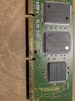
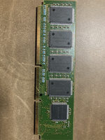
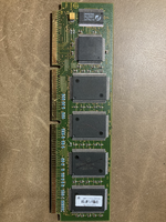
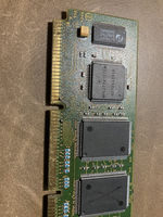
There is a cache module from the IBM RS6000 7043 p-series that would fit. It has the VCC and GND pins at the correct locations and is (at least) 66MHz capable. The cache size is 1MiB and would perfectly fit into the timeframe. The Grackle controller, the VRM and the CPU-ZIF socket are also identical to the Gossamer board.
The IBM cache-socket is a bit longer and has an addition that is seemingly not used. The cache-socket also lacks the second notch, which the cache-module has. Maybe IBM had intended to use a variety of different cache modules.

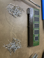
Since i live in Germany, any attempt to buy a RS6000 board to get my hands on a cache-socket have failed due to enormous prices the sellers slap on for shipping ($100 for the board with CPU and cache, $700 shipping). Im still looking into getting a cache module to (maybe) manually solder it in. It would make a comparison between G3 and 604e more interesting and maybe the onboard-cache could be used with the G3? There are hints, that a 4MiB cache module from IBM has existed but maybe that's what the extension is for on the socket.