I found a 250MB Avatar Shark drive, along with 4 disks. It has the PC Parallel Port cable. It also says on the box that SCSI interface cables for Macintosh computers are sold separately. I looked around the web, but have not found one. I guess that particular cable is probably a very rare item. Kind of an interesting drive. It looks as the disks are small HDD platters.
-
Hello MLAers! We've re-enabled auto-approval for accounts. If you are still waiting on account approval, please check this thread for more information.
You are using an out of date browser. It may not display this or other websites correctly.
You should upgrade or use an alternative browser.
You should upgrade or use an alternative browser.
Avatar Shark Drive
- Thread starter joethezombie
- Start date
I'd think it's a normal SCSI cable? Those aren't exactly rare...
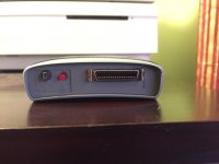
That is fantastic news! I feel a bit foolish now, not looking at the back of the drive itself... I assumed it was some proprietary connector. My attention was diverted by the bizarre printer port interface cable with power taps on differing keyboard connectors. I'll make sure to get a good look at it when I get back home.
Last edited by a moderator:
That's probably just a basic Centronics connector on the back.
It's amazing how little the Interent seems to know about those Shark drives, but unless it *says* it's a SCSI port on the back I would tread very carefully when it comes to just hooking it up to a Mac's SCSI chain. There are articles saying the external Shark was *definitely* sold in Parallel Port and PCMCIA versions, but practially no mention of an external SCSI model. (They sold an internal SCSI driver of a slightly different capacity, apparently, but it seems to be even rarer than the external ones.) What does the connector on the back look like, exactly? Is there a SCSI ID selector switch and an alternate way to power the drive other than through the keyboard taps on the parallel port connector box? If the answer to those two questions is "no" it's almost certainly not a "normal" SCSI drive.
Whatever else it might be, "Avatar Shark Drive" is a terrific name for a rock band.
Sounds like something that powers a sharknado?
Ha ha! You guys are a hoot. I have this very vivid image of an old west cattle drive going on in my head... Just replace the cattle with sharks, and the steer hands with Waterbenders. Don't forget the tornado right in the middle of it all!
So I did quite a bit of research on the shark drive. The SCSI interface cable for the Mac (if it ever did actually ship) was announced a couple of years after the drive was first introduced. This leads me to believe it is a proprietary interface, with each cable supplying a conversion. If the drive itself were SCSI, it would have had Mac support from the very beginning.
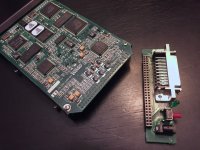
Here is the drive itself:
And here is the strange parallel interface cable:
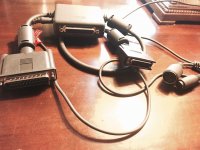
This unit is practically new in box, even has the CompUSA receipt inside. Too bad I will never find the SCSI interface for it. I do have an old Toshiba laptop running Windows95. I will try to salvage any data found on the disks. It was found in a storage shed.
So I did quite a bit of research on the shark drive. The SCSI interface cable for the Mac (if it ever did actually ship) was announced a couple of years after the drive was first introduced. This leads me to believe it is a proprietary interface, with each cable supplying a conversion. If the drive itself were SCSI, it would have had Mac support from the very beginning.
Here is the drive itself:

And here is the strange parallel interface cable:

This unit is practically new in box, even has the CompUSA receipt inside. Too bad I will never find the SCSI interface for it.
Makes me wonder if that micro centronics connector contains the direct drive interface, and the box/cable actually does the conversion. Either way, its proprietary as all get out. Maybe take it apart and look at the drive inside?
If you're lucky it will be a situation similar to the those external SuperDisk drives. The original model appears to just be a IDE drive with an adapter board similar to what you found in that photo. The cable itself provides the conversion logic to convert it from IDE to USB.
Not sure about this though. It looks it could be a modified SCSI interface with the standard cable set that converts it to the parallel interface. Though that would mean that their "SCSI" version would simply be a dumbed down cable that doesn't provide any extra conversion logic, so you would think they would have came out with that faster. But then again, there have been dumber marketing practices then that so I wouldn't put it past them.
Unlike the SuperDisk though the power connector isn't separated so if it is SCSI, it's probably not using the standard pin layout. Unless that second larger board you are showing isn't the drive it self? That or the entire thing uses a proprietary interface then you're out of luck unless you have mad modding skills or go out and find the SCSI adapter they made for it if one exists.
EDIT:
I counted the pins. It may in fact be a IDE drive + 4 pins for power. It could be perhaps using the same pin layout used for laptop 2.5 sized IDE spec which has the power pins on the same connector. Is it the same size as the 2.5 IDE interface or does it look like a full sized connector? I noticed it's even missing that middle pin (pin 20 I think?) that IDE connectors have (even the 2.5 spec version of the connector has no pin there. (usually to key the connector and prevent it from being connected backwards)
This would mean you'd need something more involved then a simple cable to convert to SCSI as in this case you'd need one of those really expensive IDE to SCSI adapters floating around. Which heck, might end up being cheaper then finding the original SCSI adapter cable to this thing.
The pin layout does make sense for a IDE interface. Pin 1 starting up top on your photo with the power pins on the other end where you see that DC in jack. (the circuit board is kind enough to label where pin 1 is. )
)
Seeing that middle pin gap in one row of the pins leads me to strongly believe it's an IDE drive with the conversion logic occurring in the cable. The daughter board much like the superdisk drives is just a pass through connector that provides an interface to the outside world.
EDIT2: I see what appear to be "MA" and "SL" jumper connectors near the top. That's for setting it to master or slave. A mainstay of the IDE interface.
Converting this to an internal IDE drive would be dead simple. (or if you want to keep it external, there are plenty of super cheap USB adapters out there for this) The only tricky part is you'll need to get the power connections correct. If it's a bastardized laptop style IDE interface but in full-sized form like those used on 3.5 sized drives, then things get a little more tricky as you'll probably have to end up Frankensteining together a custom connector/cable for it.
Either way the board makes it obvious where pin 1 is, so the IDE part of the connector is known. The only tricky part is getting the polarity correct on the power pins and figuring out pair is for the 5v connection and the 12v connection. Don't want to get those mixed up or the thing is toast the moment you plug it in. Those components near the power pins might give you an idea of which pins go to which. If you provide close up photos of that half of the connector, I'm sure someone here who knows more about this stuff then I do can probably identify which pins are for which and the correct polarity. If it's a standard 2.5 IDE interface, then they'll probably know from looking at that photo alone.
EDIT3:
I pulled the logic board off an old IDE laptop drive I have and provided a photo for comparison. The only unaccounted for pins on your drive is that extra pair on the very top labeled "EE". Which may be for that LED on the daughter board or perhaps that red button. Where exactly does that wire up to?. You can always follow the traces to see where those pins go.
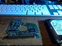
I can tell from how that missing pin is spaced that it's probably a standard IDE interface for laptop drives. The only issue is the pin size/spacing which might not be normal for the IDE interface used on laptop drives. 2.5 sized IDE interface pins and spacing is quite bit more tiny compared to the full sized version. Can't tell as there's nothing to reference scale on your photo, but it may be the full size and spacing used on 3.5 sized drives? That would be unusual for that formfactor and there may not be a easily obtainable adapter to convert it to standard IDE for 2.5 or 3.5 form factor. If it does follow normal 2.5 IDE pin size and spacing, you can probably just throw a cheap IDE to USE adapter on it and it will still work as an external drive. That all depends on the adapter you choose. You may need a Y cable to use an extra USB port for power. Not sure how much current draw that drive would pull. If it's a 3.5 sized drive, it probably pulls too much current then what a single USB port can provide.
Not sure about this though. It looks it could be a modified SCSI interface with the standard cable set that converts it to the parallel interface. Though that would mean that their "SCSI" version would simply be a dumbed down cable that doesn't provide any extra conversion logic, so you would think they would have came out with that faster. But then again, there have been dumber marketing practices then that so I wouldn't put it past them.
Unlike the SuperDisk though the power connector isn't separated so if it is SCSI, it's probably not using the standard pin layout. Unless that second larger board you are showing isn't the drive it self? That or the entire thing uses a proprietary interface then you're out of luck unless you have mad modding skills or go out and find the SCSI adapter they made for it if one exists.
EDIT:
I counted the pins. It may in fact be a IDE drive + 4 pins for power. It could be perhaps using the same pin layout used for laptop 2.5 sized IDE spec which has the power pins on the same connector. Is it the same size as the 2.5 IDE interface or does it look like a full sized connector? I noticed it's even missing that middle pin (pin 20 I think?) that IDE connectors have (even the 2.5 spec version of the connector has no pin there. (usually to key the connector and prevent it from being connected backwards)
This would mean you'd need something more involved then a simple cable to convert to SCSI as in this case you'd need one of those really expensive IDE to SCSI adapters floating around. Which heck, might end up being cheaper then finding the original SCSI adapter cable to this thing.
The pin layout does make sense for a IDE interface. Pin 1 starting up top on your photo with the power pins on the other end where you see that DC in jack. (the circuit board is kind enough to label where pin 1 is.
Seeing that middle pin gap in one row of the pins leads me to strongly believe it's an IDE drive with the conversion logic occurring in the cable. The daughter board much like the superdisk drives is just a pass through connector that provides an interface to the outside world.
EDIT2: I see what appear to be "MA" and "SL" jumper connectors near the top. That's for setting it to master or slave. A mainstay of the IDE interface.
Converting this to an internal IDE drive would be dead simple. (or if you want to keep it external, there are plenty of super cheap USB adapters out there for this) The only tricky part is you'll need to get the power connections correct. If it's a bastardized laptop style IDE interface but in full-sized form like those used on 3.5 sized drives, then things get a little more tricky as you'll probably have to end up Frankensteining together a custom connector/cable for it.
Either way the board makes it obvious where pin 1 is, so the IDE part of the connector is known. The only tricky part is getting the polarity correct on the power pins and figuring out pair is for the 5v connection and the 12v connection. Don't want to get those mixed up or the thing is toast the moment you plug it in. Those components near the power pins might give you an idea of which pins go to which. If you provide close up photos of that half of the connector, I'm sure someone here who knows more about this stuff then I do can probably identify which pins are for which and the correct polarity. If it's a standard 2.5 IDE interface, then they'll probably know from looking at that photo alone.
EDIT3:
I pulled the logic board off an old IDE laptop drive I have and provided a photo for comparison. The only unaccounted for pins on your drive is that extra pair on the very top labeled "EE". Which may be for that LED on the daughter board or perhaps that red button. Where exactly does that wire up to?. You can always follow the traces to see where those pins go.

I can tell from how that missing pin is spaced that it's probably a standard IDE interface for laptop drives. The only issue is the pin size/spacing which might not be normal for the IDE interface used on laptop drives. 2.5 sized IDE interface pins and spacing is quite bit more tiny compared to the full sized version. Can't tell as there's nothing to reference scale on your photo, but it may be the full size and spacing used on 3.5 sized drives? That would be unusual for that formfactor and there may not be a easily obtainable adapter to convert it to standard IDE for 2.5 or 3.5 form factor. If it does follow normal 2.5 IDE pin size and spacing, you can probably just throw a cheap IDE to USE adapter on it and it will still work as an external drive. That all depends on the adapter you choose. You may need a Y cable to use an extra USB port for power. Not sure how much current draw that drive would pull. If it's a 3.5 sized drive, it probably pulls too much current then what a single USB port can provide.
Last edited by a moderator:
Its definitely IDE. MA/SL give it away. The drive is highly proprietary, BUT the connector is industry standard. A regular old IDE to USB converter would work with it no problems.
The cool thing is, If there was ever a cable for SCSI, it would have basically been a SCSI to IDE converter. Probably using the Acard interface IC.
The cool thing is, If there was ever a cable for SCSI, it would have basically been a SCSI to IDE converter. Probably using the Acard interface IC.
Last edited by a moderator:
Sorry gents, been away for a bit. Thank you for the detailed analysis Apache! And you are right-- it is simply a 44-pin PATA interface, with some additional extra pins for master/slave jumpers and the eject switch.
Similar threads
- Replies
- 57
- Views
- 12K

