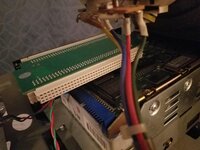
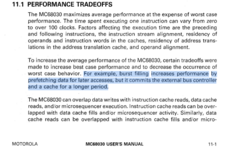
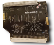
Synchr030/S is a 256MB SDRAM accelerator PDS card for the Macintosh SE/30. It combines a custom memory controller with 256MB of SDRAM to double the SE/30's memory capacity and throughput. There's no longer a need to deal with broken SIMM slot tabs, dodgy contacts or aging SIMMs. Synchr030/S provides fastest possible 2-cycle reads and writes to the 68030 CPU, making it the performance equivalent of a 256MB L2 cache that never misses.
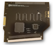
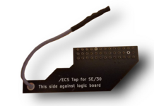
To enable 2-cycle reads, installation of the included /ECS Tap PCB is required. This small board fits over the CPU pins on the back of the logic board and routes the CPU's /ECS signal to the PDS card. This signal is not present in the SE/30's PDS connector:
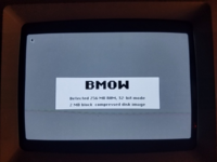
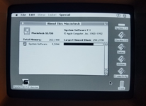
A System 6/7 extension enables fast 2-cycle access to SDRAM and expansion to 256MB under System 7 with a IIsi-derived ROM, such as the Rominator II. The extension also performs ROM shadowing, which relocates ROM-resident Toolbox routines to SDRAM, where they can execute faster. Without the extension, the card operates as 128MB of DRAM with the stock 4-cycle access time.
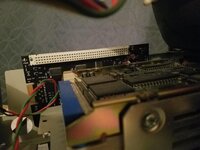
The controller operates at 63MHz, providing a 32-bit data path to memory at a maximum throughput of 31.33MB/s. Unlike the stock DRAM controller, Synchr030/S does not stall for refresh cycles, so consistent access times are guaranteed. All signals through the card are unbuffered, routed directly to the PDS passthrough connector. The two large capacitors on the board are polymer and will not leak.
Connectix Maxima is supported under System 7, which enables large, disk-backed RAM disks. SDRAM-based RAM disks typically yield 4.5MB/s with the stock CPU, faster than any SCSI device.
/STERM and /DSACK signaling options are selectable via jumper for compatibility with CPU accelerators. Compatibility is confirmed with @zigzagjoe's Interware Booster 50-SE30F clone (with /DSACK) and @Bolle's PowerCache P33 (with /STERM). Both of these accelerators benefit significantly when paired with Synchr030/S.
On the rear of the PCB, three LEDs indicate various conditions. These are visible through the SE/30's frame, and MacEffects clear case:
MacBench 3.0 Results:
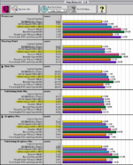
Performance summary:
MacBench 3.0 CPU score: +24%
Apple Personal Diagnostics 1.1.1 memory bandwidth: +70%
Specifications:
Power consumption: 0.43A @ 5V (2.15W) typical
Capacity: 256MB
Bandwidth: 31.33MB/s R/W
Clock speed: 62.66MHz
Slot space: C, D
Connections: SE/30 PDS male and female, expansion port, FPU LED
Weight: 123g
PCB construction: Eight layer, ENIG
Note:
Special thanks for compatibility testing, accelerator insight and feedback:
@JDW @Bolle @zigzagjoe @maceffects

 www.tindie.com


To enable 2-cycle reads, installation of the included /ECS Tap PCB is required. This small board fits over the CPU pins on the back of the logic board and routes the CPU's /ECS signal to the PDS card. This signal is not present in the SE/30's PDS connector:
A System 6/7 extension enables fast 2-cycle access to SDRAM and expansion to 256MB under System 7 with a IIsi-derived ROM, such as the Rominator II. The extension also performs ROM shadowing, which relocates ROM-resident Toolbox routines to SDRAM, where they can execute faster. Without the extension, the card operates as 128MB of DRAM with the stock 4-cycle access time.
The controller operates at 63MHz, providing a 32-bit data path to memory at a maximum throughput of 31.33MB/s. Unlike the stock DRAM controller, Synchr030/S does not stall for refresh cycles, so consistent access times are guaranteed. All signals through the card are unbuffered, routed directly to the PDS passthrough connector. The two large capacitors on the board are polymer and will not leak.
Connectix Maxima is supported under System 7, which enables large, disk-backed RAM disks. SDRAM-based RAM disks typically yield 4.5MB/s with the stock CPU, faster than any SCSI device.
/STERM and /DSACK signaling options are selectable via jumper for compatibility with CPU accelerators. Compatibility is confirmed with @zigzagjoe's Interware Booster 50-SE30F clone (with /DSACK) and @Bolle's PowerCache P33 (with /STERM). Both of these accelerators benefit significantly when paired with Synchr030/S.
On the rear of the PCB, three LEDs indicate various conditions. These are visible through the SE/30's frame, and MacEffects clear case:
- "ACCEL" LED (emerald): Indicates fast 2-cycle SDRAM access, after the extension is loaded.
- "/ECS" LED (white): Indicates activity on the stock CPU's /ECS signal. Will be off when a CPU accelerator card is in use, even if connected to the logic board.
- "FPU" LED (yellow): Indicates floating point unit access. This indicator is mirrored at the "FPU LED" through holes at the upper right corner of the PCB. An external LED header may be soldered here if desired. No resistor is needed.
MacBench 3.0 Results:

Performance summary:
MacBench 3.0 CPU score: +24%
Apple Personal Diagnostics 1.1.1 memory bandwidth: +70%
Specifications:
Power consumption: 0.43A @ 5V (2.15W) typical
Capacity: 256MB
Bandwidth: 31.33MB/s R/W
Clock speed: 62.66MHz
Slot space: C, D
Connections: SE/30 PDS male and female, expansion port, FPU LED
Weight: 123g
PCB construction: Eight layer, ENIG
Note:
- CPU accelerators may be sensitive to placement in the PDS chain.
- BMOW or other IIsi-derived ROM is required to enable 256MB under System 7.
- Basic soldering skills required for installation.
Special thanks for compatibility testing, accelerator insight and feedback:
@JDW @Bolle @zigzagjoe @maceffects

Synchr030/S by YMK Devices on Tindie
Synchr030/S is a 256MB SDRAM accelerator PDS card for the Macintosh SE/30.
Last edited:

