• Updated 2023-07-12: Hello, Guest! Welcome back, and be sure to check out this follow-up post about our outage a week or so ago.

Multiprocessor SE/30!

Trash80toHP_Mini

NIGHT STALKER
Did anyone ever do a 68K multiprocessor OS, for Workstations, Minis or whatnot? RocketShare isn't that kind of multiprocessor setup. It's software that sets up a cluster of additional single board computers within a host box networked with each other and the host over NuBus as I understand it. We've got that thread going on about the ultimate four proc PPC clone box. What OS/architecture first supported multiple processors in the micro world?


Franklinstein

Well-known member
"CLK's frequency must be stable for proper chip operation since a single edge of CLK is used internally to generate two phases..."

Obviously the 486DX2 doubles its base clock input internally, unlike the 040 which runs on two separate synchronized inputs. If the official definition of "clock doubling" is "internally doubles one input" then fine; otherwise I'm pretty sure the two sync'd inputs count because you're still ultimately operating at double the bus frequency.

The UM says "all internal timing" is based off the PCLK input, so I take that to mean 'all internal logic operates at PCLK,' not 'some parts are PCLK, some not.'

Per the UM, the 68040V is not clock-doubled; it's designed to be a very low-power chip that can clock down to 0Hz (depending on model) and completely lacks a PCLK input.

Anyway the term "clock doubled" refers to the speed at which the processor's transistors switch relative to the base frequency, not instruction throughput per base clock cycle. The UM doesn't break down the clock requirements per instruction so I have no idea what to go off of in that regard. In general you can make benchmark results convey whatever you want, depending on which tests were run and how optimized the tests were for specific hardware. If someone wants to show a comprehensive side-by-side of multiple benchmarks that count cycles per instruction for the respective chips, I would be interested in seeing it. That sort of thing is well outside the scope of this thread, though; we've derailed it slightly. 


commodorejohn

Well-known member
That's an interesting question, since the history of multiprocessing is so eclectic. The CDC 6600 rolled out in 1964 (half a decade before Unix was even a gleam in Ken Thompson's eye) and sported one or two primary CPUs and ten "peripheral processing units" (smaller, simpler CPUs whose primary function was to serve up large sets of numbers for the primary CPU(s) to crunch.) From what I read on Wikipedia, the Burroughs large systems (introduced in the early-to-mid-'60s) also supported multiprocessing. Of course, VMS made clustering a byword, but that's a bit different than true multiprocessing; I'm not sure when the VAX line actually got true multiprocessor designs. (Of course, I'm also not sure when Unix got multiprocessor support itself...?)


Trash80toHP_Mini

NIGHT STALKER
Enlarging the scope to a general discussion sounds like fun. I figured big iron had multiprocessing early on. ISTR the Mini designs my dad worked on at Prime in the late 70s and 80s used multiple processors and then microprocessors. Prime competed with DEC in the Mini era. The first to use multiple microprocessors as a unified, pipelined(?) CPU array would be what I was asking.

 
Last edited by a moderator:

Gorgonops

Moderator
Staff member
Anyway the term "clock doubled" refers to the speed at which the processor's transistors switch relative to the base frequency, not instruction throughput per base clock cycle.
And the 68040 is not *clock doubled* in any respect even if we accept that internally it "runs" at PCLK instead of BCLK because that ratio has no bearing on how fast it operates compared to some other CPU, IE, there is no "non-clock-doubled 68040" to compare it to. IE, the phrase is meaningless when applied to it. (As noted before, the old 80386DX has a pin on it that needs a clock twice the CPU's "rated speed"; I looked up the datasheet for that as well and it doesn't seem like it does anything with that clock other than divide it, but there are some weasel words about clock phases differing between the core and the bus so... ???? I didn't build it so I have *no* idea.)

Plenty of CPUs "switch their transistors" at speeds faster than the input clock. This has been a thing for a long time. (An off-the-top of my head example which I *think* is correct is the old Motorola 6809, which had two input clocks, E and Q, which ran about 50% out of phase with each other, and some operations of the ALU and bus happen in half a phase, effectively switching  at "twice" the rated clock speed of the CPU. A more recent example is the Pentium 4: parts of the ALU operate at twice rated clock speed of the CPU. Based on this why didn't Intel call the 1.4ghz Pentium 4 a 2.8Ghz CPU?)

Obviously the 486DX2 doubles its base clock input internally
I was not talking about the DX2, I was talking about the plain-old 486DX, which according to the manual internally generates multiple phases from the input clock to cadence its internal guts. IE, there are parts of plain, non-doubled 486 that could arguably be said to be operating at twice the input clock. The reason I compared this to the 68040V is because that CPU doesn't have a discrete separate pin for PCLK (it only has BCLK), it generates that "double speed" internally...

Or, maybe the 68040V doesn't use PCLK at all. The major difference other than voltage is it's a fully static design, the original 68040 isn't. PLCK might be necessary in the plain 68040 in part to handle some sort of refresh function. My ignorant guess based on some of the diagrams in the PDF is it's used to pace the pipeline but, again, no idea, I didn't build it.

Why Motorola didn't choose to advertise this clock doubling is beyond me.


Anyway the term "clock doubled" refers to the speed at which the processor's transistors switch relative to the base frequency, not instruction throughput per base clock cycle.
If you want my guess as to why Motorola didn't advertise the CPU based on the PCLK speed it's because they didn't think that *is* the CPU's effective speed. (And perhaps they also thought rating it at that speed would invite negative comparisons to the 80486... because if they counted instruction cycles in PCLKs instead of BCLKs the minimum cycle time would be 2, not one. I can just imagine the articles ripping them for that. "The 68040 claims to run at twice the clock of an equivalent 486, but the truth is more complicated than that...". If you have any doubts this would be the case, well, when the DX2s came out every PC magazine on earth was chomping at the bit to benchmark the 50mhz DX2 against the non-clock-doubled 50mhz DX and give their hot take on how the DX2 wasn't *really* a 50mhz processor.) Here is a manual that has the instruction timings in it:

https://www.slac.stanford.edu/grp/cd/soft/vxworks/doc/cpu/vme/68k/mc68040/M68040UM.pdf

The section that explains that all timings are in BCLKs is in section 10-4.(**** see below) And again, the minimum time is "1". (Note in some of the boxes where you see "1/2" that's not half a clock, that's either one or two clocks depending on some factor, like data word length.) The 486 also does some instructions in one clock cycle. Therefore whether you declare the standard 68040 as running at twice the speed of its bus or not it's effectively running at the "same IPC", where C==bus clock, as a non-clock-doubled 486.
 

The UM doesn't break down the clock requirements per instruction
(***** Actually, the thing I linked to is the same users manual you linked to, and the same information is in section 10. Use your link, it's not a terrible scan. To quote it now that I can copy-paste:

The instruction timings are based on the following suppositions unless otherwise noted:
 
1. All timings are related to BCLK cycles and are for BR = An or suppressed. For BR =
PC, 1 and 1Lclocks to the <ea> calculate and execution times unless otherwise
noted. For memory indirect postindexed with suppressed index — ([bd,BR],Xn) or
([bd,BR],Xn,od) with Xn suppressed — times are the same as for memory indirect
preindexed with suppressed index — ([bd,BR,Xn]) or ([bd,BR,Xn],od) with Xn
suppressed.
The word "PCLK" appears nowhere in section 10, and therefore no instruction timings are in PCLKs.)

In general you can make benchmark results convey whatever you want, depending on which tests were run and how optimized the tests were for specific hardware.
I'm not saying that the 68040 and 80486 necessarily "ran at the same speed", there are plenty of benchmarks out there that suggest that the 68040 was faster in the real world at least some of the time. (Again, though, you rapidly fall into a deep, deep rabbit hole with arguments about whether contemporary benchmark X is valid because reasons, etc.) It may well do a *lot* of things faster than the 486, we all know that counting Mhz is a terrible way of comparing different CPUs to each other. But I still think it's fair to throw a flag on that whole "clock doubled" claim, for two reasons:

1: Motorola never rated the CPUs based on their PCLK input, and:

2: Apple didn't start calling the 68040 a "66/33mhz" CPU until after the DX2 came out; They slapped that designation on the low-end Quadras and Powerbooks that were competing against genuinely clock-doubled 486s and it misleadingly makes it look like those computers have a different CPU than the original "33mhz" Quadras, which any benchmark will show you is not true. In other words, it was a disingenuous marketing ploy. If the 68040 is indeed faster than its "rated" speed vs. a 486 the correct course of action would have been to do the whole "Mhz Myth" thing they later invented for the G4.

Ask any Commodore fanatic and they'll talk your ear off about how the 1mhz 6502 in a 64 is "faster" than the 4.77mhz 8088 in an IBM PC, and they'll have a leg to stand on because the 6502 can execute some of the simplest of its (relatively small repertoire of) instructions in... 2? clock cycles while it takes an 8088 something like 8-11 cycles to do anything. A better way to talk about CPU performance is instructions per second, of course, but that's misleading because it matters muchly what instructions you're talking about. (The 8088 has a much larger instruction set than the 6502 and it *can* do some operations faster with a single instruction than the equivalent loop of instructions for a 6502.) If you want to say the 68040 is "more efficient" than the 80486 based on instruction counts or whatever that's legit. But that "clock doubling" thing is completely a red herring.


That sort of thing is well outside the scope of this thread, though; we've derailed it slightly. 
That is indeed true.  I just get riled up when people mention that "clock doubling" thing. ;)

 
Last edited by a moderator:

Gorgonops

Moderator
Staff member
BLAWBLAWBLAW.... If you want to say the 68040 is "more efficient" than the 80486 based on instruction counts or whatever that's legit... BLAWBLAWBLAW...
Just for the heck of it, Here is a commonly circulated rundown of reasons why the 68040 "should" be faster than the 80486 even though their best-case instruction times are the same. TL;DR, to some degree it's because you're far more likely to encounter the worse case on the 486, and the 486's ISA just kinda sucks. (Among other things its register design means it has to hit RAM more often, and that be slower.)

(The one issue I have with this article is the results of the Dhrystone and Linpack benchmarks (the latter in particular) are pretty much the least favorable to the 486 I've ever seen, to the point that I do have to hem and haw about whether the benchmark program itself might have contributed. It is really easy to hamstring x86 CPUs in ways you don't run into so much on 680x0 CPUs; for instance, issues with code alignment. x86 CPUs tolerate code at non-word offsets, which was a huge problem back when most x86 code was 16-bit and a depressing amount of that wasn't even aligned on the 16 bit words. So if it were a DOS benchmark... but, anyway. That was a real problem at the time so I suppose it's legit either way.)


GeekDot

Well-known member
Did anyone ever do a 68K multiprocessor OS, for Workstations, Minis or whatnot? 


A bit late as I just stumbled across this threat, but I know of one 68k-Monster (68020 that is): The mighty 'Suprenum'. 

Running 256 nodes, each featuring a 20MHz 68020/68851/68882 plus a vector floating-point unit from Weitek.

Its OS was called 'PEACE'... there definitely was some love for contrived acronyms ;-)

https://en.wikipedia.org/wiki/SUPRENUM


trag

Well-known member
Did anyone ever do a 68K multiprocessor OS, for Workstations, Minis or whatnot? RocketShare isn't that kind of multiprocessor setup. It's software that sets up a cluster of additional single board computers within a host box networked with each other and the host over NuBus as I understand it. We've got that thread going on about the ultimate four proc PPC clone box. What OS/architecture first supported multiple processors in the micro world?
 Massachusetts Computer sold a 68000 based mini-computer that ran some flavor of Unix back in the mid-80s.  It was very graphically oriented and had a second 68000 running its graphics adapter, IIRC.   The computer was called the Masscomp.    I think there's a Wikipedia article about it.   I used one at NASA JSC in 84 - 85. 


nickpunt

Well-known member
Round 2 of hypothetical multiprocessor Mac insanity.

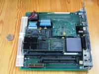
Does anyone know if the PPC 601 upgrade for LC 475/575/630 (aka Apple Power Mac Processor Upgrade or Daystar PowerCard 601 or Sonnet Presto PPC) will work in a Performa 630/640 DOS system? 

Physically it seems like this would fit just fine. These upgrades attach solely to the 68040 processor, which is readily available in the DOS version:

5319719235_002700ed5c_b.jpg

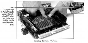
This is what one of these look like being installed on a 630 (from Sonnet's instructions):

Screen Shot 2019-02-23 at 12.32.03 AM.jpg

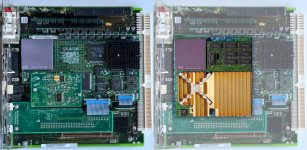
Note that the DOS version has the 68040 sitting closer to the rear of the machine, so the PPC card may not even reach the 486 heatsink. Worst case scenario, it'd just need one or two 179pin PGA sockets to increase the height a bit to physically fit. Here's a scale mockup:

Artboard.jpg

If this is possible, then we could support three different CPUs in a Mac: 68040, PPC, and 486. :D   :)   :D  

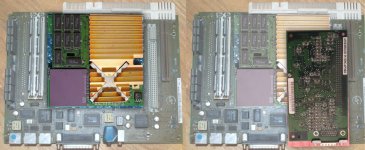
Alternately, we could start with the 575 and add the IIe card instead of the 486, making: 65C02, 68040, and PPC. Would just require a bit of eurodin stacking to physically fit:

575.jpg

Notes:

* I'm ignoring power requirements which would more than likely involve a beefier supply. 

* Oh hell, why not throw in a Sonnet QuadDoubler on that 68040 sticking off the PPC card while we're at it   [}:)]

quaddoubler.jpg

 
Last edited by a moderator:

Trash80toHP_Mini

NIGHT STALKER
.  .  .  we could support three different CPUs in a Mac: 68040, PPC, and 486
From the specs, it looks to me like you'd be running PPC OR 68040/486 chosen in dual boot config. Same for the 65C02/68040 at boot (24-bit?)  OR  PPC OR 68040/486 in 32-bit.

 
Last edited by a moderator:

Trash80toHP_Mini

NIGHT STALKER
Check that, three modes available:

PPC only

68040/486

65C02 only (never realized this combo was an either/or config.)

Since the 486 uses the 68040 socket/logic board as its I/O Bus just as does the PPC upgrade, one hack comes to mind. Wondering if it might be possible to prioritize access to the 68040 socket's I/O services to split the functions between the PPC upgrade card and the DOS Compatibility Card. The 68040 is offline while the PPC card is in operation, how does the PPC upgrade card identify itself? 6200? Might the firmware/software support be there to hoodwink the PPC card in the 630/DOS series so it thinks it's a DOS Compatibility Card for the 6200 series in a 6200 and vice versa?


nickpunt

Well-known member
This link shows gestalt IDs it shows up as:

The follow gestalt identifiers are used by the Macintosh Processor Upgrade, when installed in an eligible 68LC040-based system. When the card is active, the following gestalt identifiers are used:

gestaltPowerMac475       =104;     { Power Macintosh 475/605 }
gestaltPowerMac575       =105;     { Power Macintosh 575 }
gestaltPowerMac630       =106;     { Power Macintosh 630 }
gestaltPowerMac580       =107;     { Power Macintosh 580 }


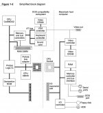
No idea about the software. The 630/640DOS is a pretty unique system. Here's the manual. Relevant diagram:

Screen Shot 2019-02-23 at 8.06.42 PM.jpg


Trash80toHP_Mini

NIGHT STALKER
If all the blocks are available and can be set up in play, I guess the only way to find out would be using two or three different boot partitions using startup disk for this kluge:

The keystone of the setup would be availability of an Apple DOS Compatibility Card and drivers for the 62xx series? There's a remote possibility those drivers might be compatible with the PPC 601 upgrade running in its sole processor setup in the 630/DOS. That's assuming it has a PPC code requirement. If the 62xx DOS card might be somehow limited to 68040 or lower code compatibility to run in the LC III PDS slot interface so much the better.

I've got a few of the REPLY DOS Cards that appear for the 62xx series. They plug into the LC III PDS and the Video connector slot at the back of the board. Dunno much about 'em yet, but if they're compatible with the 630 series that could make for better compatibility than even drivers for an APPLE DOS Compatibility Card? Physical compatibility is another story entirely, but elevator shoes might just work? Installation would need to be done through the lid with logic board drawer already installed. FM/TV tuner in/Video out board cage would need to be removed with the former out of the equation and the latter re-positioned.

/caffeine deprived silliness mode

Googlefu test: locating info and drivers for the REPLY DOS card would help a lot here:

Cards were distributed by Radius

(c) REPLY CORP 1996

Processor Board to PDS w/Mac Video out: Assembly 05012800 B

I/O Daughtercard to Video Slot in(?) and octopus cable out Assembly 05012700 B

Interesting thing here, the REPLY card has what's probably a far more capable S3 Graphic Chipset and connection to the Mac Video Out slot would appear to be a passthru for displaying a Mac Video window within the DOS card's main Windows/VGA output display at higher resolution?


olePigeon

Well-known member
Radius had big plans for multi-CPU configurations.  I think that was the point of their ill-fated Skylab project.  You'd stick a bunch of Rocket IIs in an external NuBUS box, then use it as a self-contained rendering farm.  PowerPC made it a moot point.

I wonder if they had plans to make it compatible with Symbolics.

 
Top