• Updated 2023-07-12: Hello, Guest! Welcome back, and be sure to check out this follow-up post about our outage a week or so ago.

Multiprocessor SE/30!

nickpunt

Well-known member
"Scientists were so preoccupied with whether they or not they could, they didn't stop to think if they should"
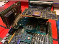
IMG_4757 (1).jpg

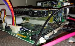
In all seriousness though, has anyone ever attempted to put two accelerators in an SE/30? For example, a socketed powercache and a turbo 68040:
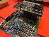
IMG_4768.jpg

I have no particular desire to be the first to attempt it as I don't want to see two extremely valuable parts go up in smoke, but my understanding is the Turbo040 can be enabled / disabled in software, so if this configuration worked electrically & in drivers, you could have the best of both worlds in software compatibility, given some software works better on 030s than 040s. My guess is daystar software would be rather confused by this whole arrangement, but who knows?

 

Trash80toHP_Mini

NIGHT STALKER
Off the top of my head, you'd need something along the lines of RocketShare. It runs multiple processors in a 68K Mac as if they were different Macs in the same box booting off copies of the host's ROM in RAM on each Rocket. That way they can could share processing tasks with the host and each other, communicating via LocalTalk over NuBus.

You've got two processors (accelerators) in that pic that take control of the system bus. They shut down the Logic Board CPU and neither plays nicely with others. They act pretty much the same as a Rocket  under RocketWare in Accelerator mode.

@olePigeon, did you have a Turbo040 or the like and a Rocket in your IIci Running under RocketShare?

/Jurassic Park [;)]

 
Last edited by a moderator:

Gorgonops

Moderator
Staff member
Devil's advocate-ly wise I'm not sure why this necessarily *wouldn't* work given the socketed CPU upgrade removes the original one. Presumably there's some line on the PDS connector that allows the slotted accelerator to steal control of the CPU bus generally (IE, put the socketed cpu "to sleep"); if *any* other type of PDS card uses this same busmaster line to halt the main CPU then presumably the socketed accelerator would need to honor it. Therefore... maybe it would be perfectly okay to have the socketed accelerator present with the Turbo 040 plugged in? But...
 

I don't think you can enable/disable the Turbo 040 in software.
This PDF seems to confirm that. The control panel has all kinds of options for dumbing down the 68040's cache to try to make it more compatible with troublesome older software, but I don't see a "disable the card entirely" button. Lacking that then all you'll get out of having the socketed accelerator present is more area for dust to settle on.


Von

Well-known member
What card is plugged into your socketed SE/30 Daystar in the top photo?

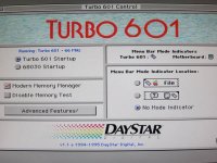
Although it doesn't work in a SE/30, the Daystar Turbo 601's control panel allows it to boot to 030 or the 601. I wonder if you could boot this insanity:

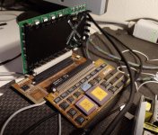
2018-11-15_15_06_11.jpg

That is a IIsi cache card with the 601 in the pass through and an 030 50mhz going in the cache slot then into the IIci on the bench:

2018-11-15_15_07_06.jpg

I am not willing to try this.  In addition, the cache card didn't engage as it was bumping into the RAM. That could be sorted with one PDS riser...


Gorgonops

Moderator
Staff member
Off the top of my head, you'd need something along the lines of RocketShare. It runs multiple processors in a 68K Mac as if they were different Macs in the same box...
Note of course that the only reason Radius Rockets can do this is the card itself is essentially a whole computer with its own onboard RAM sockets, etc. When a Rocket is running as a simple "accelerator" (IE, not using RocketShare) it technically still delegates some I/O functions it can't do itself through Nubus busmastering to the onboard CPU.


nickpunt

Well-known member
@Von the first photo is just a joke, it's a Turbo040 -> daystar IIcx adapter (fake) plugged into -> socketed daystar board. And then another daystar 030 accelerator -> micromac PDS adapter -> MacCon. I tried for maximal ridiculousness :)

@Gorgonops this is what I was thinking - the socketed daystar just works without any drivers or anything. 030 accelerators don't seem to modify the ROM in any way (hence they can use the ROMinator II no problem). Any non-030 accelerators both modify the ROM and have some degree of software control, and there's precedent to having software disable accelerators entirely.

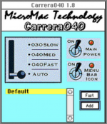
MicroMac Carrera040 has a control panel with a switch to turn it to 'slow' which disabled the processor. In the FAQ, they state:

Q: I currently have a FPU installed, can I still use this FPU once I installed the Accelerator?
A: No, once the Accelerator is active, it will disable the CPU and the FPU you have on your logic board.


Screen Shot 2018-11-15 at 4.21.08 PM.png

Turbo601 as @Von points out can be disabled.

m196192525.3.jpg

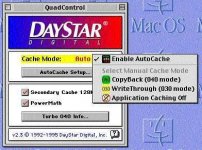
Turbo040 has Daystar QuadControl you can disable application caching, PowerMath, Secondary Cache Control. Maybe all of those together would potentially just disable the accelerator entirely? Sometimes software is written in a way that doesn't explain its exact function, and QuadControl's options might be one of these situations.

14-2.jpg

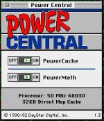
One interesting thing is that there's different software for 030 and 040 daystar accelerators. The 030 uses PowerCentral, while the 040 uses QuadControl. PowerCentral has two on/off switches for cache and FPU:

powercentral.jpg

This doesn't suggest the accelerator CPU can be disabled. In the case of the socketed SE/30 powercache, that would lead to not having a CPU at all, so probably a good idea not to have that option  :)  

Order of operations

1. Electrical - can they be plugged in together without magic smoke?

2. CPU Bus - does the computer know which CPU to send stuff to?

3. Drivers - is it possible to change options in the 040 such that disabling those will fall back to the 030?

#1 my guess is it won't make smoke.

#2 seems kind of suspect. but, given only the 040 is modifying the ROM, it may mean its pointing to the 040 first.

[SIZE=1.4rem]#3 raises the question whether disabling the 040 FPU/cache falls back to the PowerCache 50mhz FPU/cache, or simply disabling both accelerators FPU/cache. [/SIZE]Probably[SIZE=1.4rem] depends how the control panels are written. In fact, the computer may refuse to boot simply if you have both QuadControl and PowerCentral active. [/SIZE]

But I'm still hesitant to run the experiment :p  

 
Last edited by a moderator:

Gorgonops

Moderator
Staff member
Sometimes software is written in a way that doesn't explain its exact function, and QuadControl's options might be one of these situations.
The explanation of the options in the documentation doesn't read to me like it under any circumstances completely disables the '040. (For instance, it specifically says that "030" mode means setting the '040's cache to write-through mode, "Powermath" involves a software module to substitute for some of the routines in Apple's SANE library... etc.) It may well be that whatever method it uses to put the motherboard CPU to sleep is hard-wired. IE, if the card's installed the "disable" switch is held down.

MicroMac Carrera040 has a control panel with a switch to turn it to 'slow' which disabled the processor. In the FAQ, they state:

Q: I currently have a FPU installed, can I still use this FPU once I installed the Accelerator?
A: No, once the Accelerator is active, it will disable the CPU and the FPU you have on your logic board.
I'm not 100% certain that the acellerator's CPU is actually disabled on this one either, and the wording of the FAQ is kind of nebulous. (It mixes the words "installed" and "active". Can it be "installed" but not "active"?) Are you certain that its "030" mode isn't the same as the Daystar's, IE, it actually means the 040 is running with all caching disabled?

b) does disabling the 040 FPU fall back to the PowerCache 50mhz FPU, and same for cache?
It doesn't look to me like the 040's FPU is actually disabled by turning off that "Powermath" option, it just changes the SANE pathways.

So far as I'm aware you can't use a 68881/2 with a 68040 under any circumstances other than the rarely used "memory-mapped peripheral" mode the chip also supported, so I can't imagine any circumstance under which a 68040 accelerator of any sort would make use of an FPU sitting in the socket of an upgraded machine.

 
Last edited by a moderator:

joethezombie

Well-known member
Well the Carrera040 will happily exist in an SE/30 with the IIsi adapter, remaining inactive.  But once the INIT and control panel are placed, the system bombs with an address error.

 
Last edited by a moderator:

nickpunt

Well-known member
@Gorgonops this reminds me of something I read the other day about the 040 and the 68882:

https://en.wikipedia.org/wiki/Motorola_68040

Unfortunately, the 68040 ran into the transistor budget limit early in design. While the MMU did not take many transistors—indeed, having it on the same die as the CPU actually saved on transistors—the FPU certainly did. Motorola's 68882 external FPU was known as a very high performance unit and Motorola did not wish to risk integrators using the "LC" version with a 68882 instead of the more profitable full "RC" unit. (For information on Motorola's multiprocessing model with the 680x0 series, see Motorola 68020.) The FPU in the 68040 was thus made incapable of IEEE transcendental functions, which had been supported by both the 68881 and 68882 and were used by the popular fractal generating software of the time and little else. The Motorola floating point support package (FPSP) emulated these instructions in software under interrupt. As this was an exception handler, heavy use of the transcendental functions caused severe performance penalties.


Trash80toHP_Mini

NIGHT STALKER
Note of course that the only reason Radius Rockets can do this is the card itself is essentially a whole computer with its own onboard RAM sockets, etc. When a

Rocket is running as a simple "accelerator" (IE, not using RocketShare) it technically still delegates some I/O functions it can't do itself through Nubus busmastering to the onboard CPU.
Exactly, a Rocket is a "Mac" in its own right once the host ROM is copied into its RAM at which point it reboots running under either RocketShare in its multiprocessor mode or RocketWare in Accelerator mode as the only "Mac" with the host CPU relegated to I/O duty like the pair of 6502 CPUs on a IIfx board.

@nickpuntI figured your pic with the IIcx adapter was for shiggles and gits, but held my tongue. [:)] I think it's wonderfully over the top!

Interestingly, the Universal PowerCache in its adapter worries not about whether the 68030 socket on the SE/30 board is inhabited. It yanks on some line or other (ask Bolle) in the case it is and runs just fine sans mobo processor in the case that it's not. That makes the CPU socket a fabulous PDS wedge for installing a board of some kind ot other at some point.

Thanks for the FPU info, nick, I hadn't seen it explained that way. All I'd read was that the CoPro on the 68040 die was a less capable subset of discrete 68881/68882 function. Incompatibility was a good call, on the other side of the fence, I couldn't afford a 386DX system when CorelDraw came into vogue. So I bought a 386SX board that had a socket for the 286(?) generation FPU. Crunched every number vectorization routines and CorelDraw threw at it right nice! 68LC040/68882 combo could have kicked some serious number munching butt had Motorola not headed that combo off at the pass.

 
Last edited by a moderator:

Franklinstein

Well-known member
Motorola did a bunch of obnoxious crap with the 040. Some of it, such as changing the processor bus to a type that is incompatible with the 030 and previous chips, may have been done strictly for performance or efficiency improvements rather than to preclude the use of older, cheaper support chips (though I more suspect it was the latter). Others, such as blocking the use of an external 68882 with an LC040, were done simply to prevent people from upgrading their existing LC040 chip with an external part; instead you have to buy an entirely new 040 to gain an FPU that is only mostly compatible with the 68882. Of course, since the 040 was internally clock-doubled and an external 68882 would not be (so it would be an internally 50MHz 040 redirecting instructions to a 25MHz external FPU), it would not have been an ideal solution anyway. It would have been nice if the choice was presented to the customer, though.

To be fair, Intel didn't really offer a 487 upgrade option for their chips either: the rarely seen 487 was a full 486DX in a special socket that simply disabled the existing 486SX (which I assume was soldered rather than socketed in these arrangements).

I believe the 040 could run in a multiprocessor arrangement with the use of additional Motorola support chips. Of course nobody ever really bothered with it because it was crazy expensive and required a lot of board space in addition to whatever software support was required to make it work properly.


Gorgonops

Moderator
Staff member
course, since the 040 was internally clock-doubled
No, it isn't. The 68040 takes an external clock twice the internal, not the reverse. (Like a true clock doubled chip, like the 486DX2; interestingly enough the 386DX also took a double speed clock.) Very little of the 040 effectively runs at the higher speed. This idea that it's clock doubled is the result of some very misleading advertising from Apple that quoted the raw clock input to make the later consumer 040 machines look directly comparable to the DX2, which has swept the PC world by storm by 1993-ish.


Franklinstein

Well-known member
According to the user manual (pg 7-1):

"The M68040 uses two clocks to generate timing: a processor clock (PCLK) and a bus clock (BCLK). The PCLK signal is twice the frequency of the BCLK signal and is internally phase-locked to BCLK. PCLK is also distributed throughout the device to generate additional timing for additional edges for internal logic blocks and has no bearing on bus timing. The use of dual clock inputs allows the bus interface to operate at half the speed of the internal logic of the processor, requiring less stringent memory interface requirements. Since the rising edge of BCLK is used as the reference point for the phase-locked loop (PLL), all timing specifications are referenced to this edge"

So a part marked XC68040RC25B receives a 25MHz clock for the bus, and a second 50MHz clock for internal use. On most Macs, the host machine typically has a (in this example) 25MHz oscillator that feeds the 040 the 25MHz BCLK signal directly and a PLL circuit of some variety doubles the clock to 50MHz for the PCLK input. On others, such as the PowerBook 5x0, the host's oscillator is 1/2 bus speed (in this example the crystal is 12.5MHz), so a PLL circuit doubles this to 25MHz for the BCLK and doubles it again to 50MHz for the PCLK.

Why Motorola didn't choose to advertise this clock doubling is beyond me. Maybe they didn't ask marketing. Maybe they wanted to make it easy for system designers and integrators by referencing only the bus clock. Maybe they didn't think about it. Maybe their documentation was screwy. Either way, the only chips marked as doubled are the QFP models in PowerBooks: those say 50/25MHz or 66/33MHz on them.


Bolle

Well-known member
I wonder if you could boot this insanity
No. Pinouts are drastically different between „Cache“ slot and PDS slot. Trying this in either the IIsi or IIci will result in shorting 5V to ground at best probably killing things in the process if the PSU doesn‘t turn off quick enough.


Bolle

Well-known member
I'm not 100% certain that the acellerator's CPU is actually disabled on this one either
It is disabled and control is handed over to the onboard 030.

The way the IIsi adapter for the Carrera is wired up also suggests that. /BR, /BG, and /BGACK are wired up right between the main PDS connector and the accelerator slot.

The Mac starts up with the main CPU and the C040 takes over once the INIT loads. You can see the three control lines toggling accordingly everytime you switch the C040 on and off in the CP.

On the Daystar adapter for the PowerCache and T040 the /BR line is tied to the GAL which disables the onboard CPU as soon as there is an accelerator present in the cache slot.

The DiiMo adapter for the SE/30 pulls down /BR disabling the logicboard CPU completely as well. That’s why the Mac won’t start with only the adapter in place but no accelerator installed.

The IIsi adapter for the T601 again is wired up different again to support switching the /BR line to enable or disable the logicboard CPU.


Gorgonops

Moderator
Staff member
According to the user manual (pg 7-1)
If you check page 86, section 6.2.1 of the 486dx datasheet on archive.org it says this about the clock input:

... CLK's frequency must be stable for proper chip operation since a single edge of CLK is used internally to generate two phases...

IE, it seems to do something very similar to the 68040V because for various reasons it needs this higher frequency to cadence certain parts of its internal circuitry, but this doesn't effectively add up to the core being "double clocked" compared to its bus. There are a lot of nerdy arguments on mailing lists about what the significance of the PCLK/BCLK ratio *really* means in the 68040, but from everything I've seen the instruction timings of both the 040 and the 486 are based on how many "BCLKs" an instruction takes and neither CPU can do any full instructions in fewer than one.(*)

(I did see one discussion that claimed that there were parts of the 040's FPU that can complete instructions in a non-integer number of BCLKs, IE, that bits of it do run at full PCLK speed. But the whole CPU is not functionally on par with a DX2, which can do two of all the single-cycle instructions a DX can do in one bus cycle.)

 
Last edited by a moderator:
Top