• Updated 2023-07-12: Hello, Guest! Welcome back, and be sure to check out this follow-up post about our outage a week or so ago.

Designing a portable RAM card

Elfen

Well-known member
Yeah, dealing with China can be expensive in shipping costs and shipping time (up to 6 weeks or more to go through customs? Sheesh!) But they are cheap otherwise.

TechKnight, copyright your design (send 2-self addressed mailed planes to yourself and open one up to see it and keep the other sealed until a "judge needs to see it," and keep both together) and then get an application to send a copy to the Copyright Office at the Library of Congress. Last time I had something copyrighted by the LoC was in the 1990s and cost $14, I don't know what it is now. I understand that you are doing this for the community and all, but its best to protect your ideas. It's nice to have that "by © year" with your name on it on what you put out.

 
Last edited by a moderator:

aplmak

Well-known member
I can't even wait!!!!!!!!!!!!!!! You are the bomb Techknight!!!!!!!!!!! I may buy 8 if I can afford them... :) and if you produce enough.. :)


techknight

Well-known member
As long as I dont find any more errors ill run the boards.

Get a BOM together and figure out the cost per board from there.

Hey trag can you message me the chip prices so I can factor that in.

 
Last edited by a moderator:

aplmak

Well-known member
PCB Express here in the US and Shennan Ckts in China.. High quality.. shennan takes gerber files and will convert and PCB express requires you draw with their software.. Which is free.. A friend uses these guys


techknight

Well-known member
I used to use ExpressPCB but I quit because its proprietary. Much easier than eagle though, but i rather use something that renders industry standard files. 

plus expressPCB is very expensive. 

I was using iTead with prototype runs, because it was cheap. but one of the guys split off and started his own thing, and i got a quote from him. 


techknight

Well-known member
BTW, the diagnostic LEDs will likely be programatically hooked up to each chip select. So youll see them flash during the RAM test, or during read/writing in that RAM space. 


uniserver

Well-known member
flashing lights makes it look more important!   :)

batman_burroughs_b205.jpg.78a522d203e04d29368a2b75c0cee239.jpg


techknight

Well-known member
Whoops. Almost royally screwed up. Got to make a design change. 

These are 2MB chips. the on-board RAM is only 1 MB in size, and the decoding to external address space starts at 2MB. Problem is, the New RAM is 20 bits in size, while the original is a total of 19 bits in size. So, if I leave A19 of the toshiba RAM hooked into A20 of the original addressing space, that would kill off the first 1MB on my toshiba chip, basically wasting half the chip, as A20 would be high when moving into external addressing. Since A20 is routed to the toshiba chips, well yea.... 

So, I am going to have to break off A20 from the RAM. Leaving the RAM only accessing in 1MB chunks. Then, move A20 to the CPLD and do some 1-2 decoding to use the full address space. 

Wow... good thing I caught that. Doing the CPLD work is what made me think of this. 

This is precisely the reason that when using memory modules in computers, they all have to be "equal" 

Elfin: Even if I did copyright it, whos got the money to hire a bunch of lawyers and court proceedings to fight an infringement? I dont, so who cares? Plus this is strictly a niche market with a small yield so it doesnt really matter. 

 
Last edited by a moderator:

techknight

Well-known member
CPLD code is done, now its just a matter of waiting for the PCBs, assembly, JTAG programming, and test... 


techknight

Well-known member
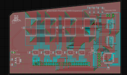
Ordered the PCBs, which pretty much depleted my budget. 

Soon as I get some extra cash, I can order up the parts from digikey to finish the boards. 


Paralel

Well-known member
...(send 2-self addressed mailed planes to yourself and open one up to see it and keep the other sealed until a "judge needs to see it," and keep both together)...
I can say, with true and absolute certainty, that this hasn't been accepted as evidence in patent court for at least 40 years, if not longer.


techknight

Well-known member
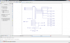
Here is my CPLD code in a nutshell: 

Chip Select/Bank Select Signals.
A20, A21, A22, A23 Address line decode. The chip is hooked up between A0 and A18, or A1 to A19 if you look at the portable bus. 

Base RAM:
0000 = No chip selected, all lines off = 0

Extended RAM:
0001 - Chip 1 Select ON, Lower Bank ON = 1
0010 = Chip 1 Select ON, Upper Bank ON = 2

0011 = Chip 2 Select ON, Lower Bank ON = 3

0100 = Chip 2 Select ON, Upper Bank ON = 4

0101 = Chip 3 Select ON, Lower Bank ON = 5

0110 = Chip 3 Select ON, Upper Bank ON = 6

0111 = Chip 4 Select ON, Lower Bank ON = 7
1000 = Chip 4 Select ON, Upper Bank ON = 8

When I say Upper/Lower bank, I mean just toggling A20 high or low. Since the macintosh portable has base RAM at 512K-Word, or 1MB, I decided to break the expansion down into 1 meg chunks as well. Since the toshiba chips are 1M-Word, or 2Mbytes, just deciding where A20 is determines if I am working with the first 512kword, or the second 512kword. 

 
Last edited by a moderator:
Top