• Updated 2023-07-12: Hello, Guest! Welcome back, and be sure to check out this follow-up post about our outage a week or so ago.

Another IIci ROM hack

dougg3

Well-known member
The Iici (and the other computers) have a 25mHz bus and a MC68030 CPU. Why can they read perfectly fine to/from ROM/RAM/CPU/HDD, but we need a 100 MHz FPGA to do the same? I've never seen a 3rd party add-on card that needs a FPGA with a MHz ratio of 4:1 to the host computer to work before(??). I'm not sure if I understand this.
I wasn't analyzing how fast of an FPGA it would need (I'm actually clueless on that front). I was analyzing why a microcontroller would be a bad idea and an FPGA would probably be required. The FPGA will have an easier time catching the hardware signals on the bus saying "a write happened" or "a read was requested". A microcontroller running at the high clock rate of 100 MHz would still be pretty stressed at high data rates just handling the accesses and decoding the addresses, while an FPGA should be perfectly capable of handling it -- that's what my big write-up was about.

Is it possible that the microcontroller can handle it? Maybe -- definitely not in the ROM SIMM slot because there's no mechanism for the card to slow down read accesses to it, but it might work in a PDS slot where the PDS card has to acknowledge that a read has completed as I'm seeing with bbraun's latest hardware work. But with the idea of a ROM SIMM card with a microcontroller in it, I'm just saying that a microcontroller is a bad idea and an FPGA is the way to go.

 

Trash80toHP_Mini

NIGHT STALKER
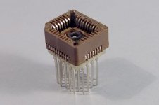
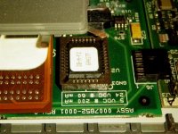
That article describes *exactly* what I do to the PLCC sockets on the 2 MB SIMM :)
LOL! I thought you'd get a kick out of that one. [;)] ]'> I figured it was a good reference for this monster thread.

You have to use single-supply EEPROMs/flash chips -- it won't work with chips that need a high programming voltage. It has to be a chip that only needs a single 5V supply, like the Am29F040 or the SST39SF040 (and their smaller brethren). Hopefully this doesn't limit the options too much...
1) this is where you've lost me, I've never had to spec ICs and I've never shopped for any I couldn't get at CrapShack.

2) I'm only familiar with the ROM packages for the systems I mentioned, suggestions for any others ought to be made now.

IOW . . . HELP!!!!! 8-o can someone (besides DQ, we're making this a community development project after all) do the research on any different ROM packages that it would be good to add to this board? Checking parts availability per DQ's spec for the ones mentioned above, I've never determined the IC package type for the DuoDock+ ROM. I've had the spec for the MiniDock/DuoDock ROM on hand for a few years.

< . . . slurps down the beginnings of second cup of coffee, bops wetware reset button. :scrambled: >

I may be overdoing/under-over-thinking this . . .

The first thing I'm going to add to the PCB will be the pins for the DIP socket equivalent of the expansion headers on DQ's programmer. Standard form factor (not pinout) adapter modules can be user fabbed for additional ROM types as needed.

I still want to do socket pads for a basic set of Mac ROM packages . . . so . . . help!!!!! :I


bbraun

Well-known member
The first thing I'm going to add to the PCB will be the pins for the DIP socket equivalent of the expansion headers on DQ's programmer
AFAIK, 29F040 (what I'm using) is the DIP equivalent.


Trash80toHP_Mini

NIGHT STALKER
Pictures work better for me than .TXT, so:

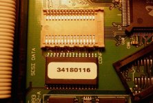
In order to add pads to the extender board to create a ROM SIMM adapter when the extender is plugged in B@$$@ckw@rd$. These are the packages I've babbled about above. The old 28 pin EPROM socket's not a problem, I may even have one or two ZIF Sockets stashed away somewhere. All the early DeclROMs for NuBus Cards and a few peripherals used this DIP Package

Duo MiniDock DeclROM _________________________________________

minidockdeclromfront.jpg

This appears to be a lower profile SMT socket = too hard to work with . . . :p

MiniDock DeclROM thru-hole socket _____________________________

minidockdeclromprotosoc.jpg

This is what I'm looking for, if not its ZIF equivalent. I don't need the machine pin extended wire wrap adapted version, the socket pictured is a standard thru hole socket mounted to an adapter PCB. This is the wire wrap equivalent of the "Machine Pin Hack" I've been proposing in the SuperIIsi thread.

DuoDock DeclROM______________________________________________

duodockdeclrompowerhack.jpg

DuoDock+ DeclROM_____________________________________________

ddiideclromtopzif.jpg

Now that I'm looking at it again, is this a ZIF socket for the same SMT package in the DuoDock DeclROM pic above?

My eyes stopped working after counting the socket connections on an Apple Video Card24AC to compare them with the MiniDock DeclROM . . .

. . . yep, they're the same package! [:D] ]'>


Trash80toHP_Mini

NIGHT STALKER
http://www.jameco.com/Jameco/Products/ProdDS/104012.pdf

Thanks, Sancho! That's one more, but I'll still put the big'ole .01" DIP socket (a pair of 32s I have in stock) on the board in constricted, alternating pin for pin series with the SIMM expansion headers customizing. That'll make for easier fcustomization of adapter-adapters as well. :approve:

I'll need to have the pinout conversion from your EEPROM to the Programmer's expansion headers for the necessary switcharoonies.

The same is true for the rest of the pinout conversions, my brain doesn't work that way, this is a graphic art project for me, I've always had a hardware/software guy feed me the pinouts and my noggin converts that into postscript paths in illustrator. Matter of fact, I'm toying with the notion of having a buddy of mine who's still in the sign business up in NYC do the board's edge connector thicknessing, "etching" and drilling for me on one of his engraving machines. [}:)] ]'>

p.s. I counted pins in the pics above and it looks to me like the 'Dock & the 'Dock+ use the same ROM package: now for sourcing that ZIF socket to retrofit my DuoDock MLB and, preferably, in thru hole as well for the extender/adapter.


techknight

Well-known member
The Iici (and the other computers) have a 25mHz bus and a MC68030 CPU. Why can they read perfectly fine to/from ROM/RAM/CPU/HDD, but we need a 100 MHz FPGA to do the same? I've never seen a 3rd party add-on card that needs a FPGA with a MHz ratio of 4:1 to the host computer to work before(??). I'm not sure if I understand this.
Because the FPGA of today is the VLSI of back then. its glue logic, all it is. And its programmable while VLSI was masked. Nearly every PDS/nubus card you see or has been made has PAL/GAL or some form of VLSI on it. THIS IS WHY...

So you replace PAL/GAL/VLSI with an FPGA. and you can take over all the roles with the single IC as things are much more highly integrated today than they were back then.

and 100mhz means thats the speed the logic is capable of running at.

sure you can do everything in discrete glue logic, if you want 30 ICs on your card.


Trash80toHP_Mini

NIGHT STALKER
Speaking of the discrete IC days of yore, that's the era of the cabling I've decided is plenty good enough today, with one little knuckleball thrown in!

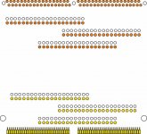
ROM_SIMM_Extender_01.2p.jpg

I was over-designing the SIMM Card portion of the extender. Now I've reduced the complexity to just 40 pin and a 28 pin DIP Plugs for old-school ribbon cable . . .

The knuckleball is just one litlle hack! [}:)] ]'> I'll be terminating the second of each pair of plugs using the opposing ends from the first dip plug after I've installed the first DIP Plug installed in the middle of a double length cable . . .

. . . then open up the lid of the first DIP Plug and cut a chunk out of the very middle of the cable between the first dip plug's forks. [:D] ]'>

Just tie the unused cable wires to ground and voila! Extender cable with alternating ground shielding . . . on the cheap! :approve:

edit: HEH! p. 38 rollover post! [:eek:)] ]'>

. . . forgot to mention, the SIMM is currently oversized by the black delineated amount. I was in a hurry to get the graphic done, so I miscounted pads. Now I've got room to drop the sockets down, maybe skootch 'em together a bit, to fit them easily within the outlines of DQ's SIMM. The extended lines run off to the ZIF Socket DeclROM programmer adapters and the female end of the extender, with the SIMM Slot.


techknight

Well-known member
oh boy. lol. signal ring and Crosstalk-galore :)

In order for this to work properly, you'll need to impedance match both ends, and rate it for the speeds being used.

Same thing as trying to run a 536ohm antenna in a 50ohm connection. noooot going to work very well.... Your going to need LPF impedance matching at both ends.


Trash80toHP_Mini

NIGHT STALKER
Properly? Who said anythin' about it being properly done!?!? }:)

No crosstalk with alternate ground line hack, the rest is very iffy, but it's just a down and really dirty proof of concept design. It should pass repetitive reliability testing with at least ten inches of cable, even at the IIci's clock, if not a bit more. It worked back in the day with longer cables without the alternate ground lines . . .

. . . and it makes a GREAT RFI amplifier. :eek:)

n.b. PCI extenders are available with 5-6 inch lengths of ribbon cable. The longer one I have has zero electronics on it, doubled cables for alternate grounding and seems to work just fine.


tt

Well-known member
JT, I think I missed something, what are you up to with the extender? :?:


trag

Well-known member
jt, to answer your thickness question.

The old SIMM thickness is .050" or maybe .047". Typical PCB or copper clad board, these days, is .063" or maybe .0625", whic his also modern DIMM thickness, I think.

The SIMM sockets of yore have pins on both sides, even though the pads on opposite sides of the SIMM are common with each other. So it doesn't really matter which side you grind down, as long as one side is still available to make contact with the socket pins.

Grinding the pads off of one side of the board can't be good for reliability though. It's better to get the proper thickness copper clad board in the first place. Are you in imminent danger of etching something yourself? With the prices at Seed Studio, you're almost always going to be better off using them. Especially since making vias is a time consuming, finicky pain.


Trash80toHP_Mini

NIGHT STALKER
The way I understand it, is that I'm taking the very low road to test the feasibility of moving the programmed ROM SIMM from the socket on the mobo to the socket on a card in the FDD bay. DQ seems to be exploring the high road possibility of using an FPGA to connect to additional neat stuff, whether on a larger(?) ROM SIMM or on the end of a cable as I had suggested.

Real estate on an enlarged ROM SIMM will be severely limited, especially for the SE/30 crowd. Moving additional circuitry, even the ROMs themselves to the FDD Bay seems like the best choice to me. If we're gonna do an SD Card or any other modern, removable I/O hack, having it near the FDD Slot is a no-brainer as far as I'm concerned.

The graphic that got you laughing is the current iteration of the dummy SIMM end of the extender.

This one gives a better picture of the two halves, the board will be cut cut across the middle.

Adapter export 3.jpg

When I did this quick study, I thought I'd need to use three standard IDE cables and headers for them at each end of the testing units. When I researched the newer ATA cabling, I cut it down to two connectors/board. I'm going to take a nap and fire up Illustrator 8 again tonight.

1) Move the dip plug sockets together and lower on the board to bring it in line with DQ's ROM SIMM form factor.

2) Continue the traces on to the Dip Plug sockets and SIMM Slot end of the extender Cable.

3) Continue those traces on to a 64 position machine pin socket for homebrew programmer adapter development.

4) Continue those traces on to sockets for:

________ the yet to be identified DuoDock ROMs . . .

________ the PLCC ROMs for the MiniDock and my Radius VidCards . . .

________ bbraun's suggested EEPROM package . . .

________ the 28pin EPROMs used on most early Cards and peripherals . . .

________ whatever other suggestions come up . . .

________ and just maybe . . . the friggin' kitchen sink! [:eek:)] ]'>

Other than some patch wiring for the adapter connections, It's pretty much a single sided board that doesn't need any plated thru holes . . .

. . . should get three sets ganged on a 12'" x 12" blank . . .

. . . dunno, we'll see, I've got a couple more notions rattling betwixt the earlobes, ATM. :scrambled:


tt

Well-known member
I see... sounds like a good idea for a feasibility study. I'm not knocking any ideas around here, most experiments have the potential lead to new discoveries or ideas. :b&w:

The extender could also relate to the idea of extending the CPU socket or PDS slot for the Daystar crowd, right?


Trash80toHP_Mini

NIGHT STALKER
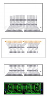
ROM_SIMM_Extender_05.2p.jpg

Ok, gang, here's the concept study for the extender project as it now stands.

Criricism-n-suggestions of every type are encouraged and will be much appreciated. :approve:

Input signal flow is represented in the diagram as from bottom to top and each cards is shown as a discrete unit. The actual layout is still single sided. for a one of the three ganged cards in a row of the three triplets on the 12" x 12" copper clad FRP from CrapShack I'm still hoping to find in one of the boxen. The top card will be rotated 180 degrees so the edgecard connectors are on the opposing side of those on the bottom card. Other sourcing suggestions for inexpensive fab on a one square foot, max size, blank will be considered.

______________________________________________________________________________________________________

The top card is a parallel, peripherally related, development that's a gimme in the production process. It's intended to make adapting dougg3's programmer board for use in building "standard" format adapters for individual or ganged ROMs in alternate IC packaging by the traditional process. The loose traces will lead to the four different socket types discussed earlier, wire wrap or soldered patch wiring will be necessary unless I move to a double sided, plated thru hole process on a blank of the proper thickness. I'm assuming that this will be prohibitively expensive, prove me wrong PLEASE!. Funds for the toy account are unbelievably tight for the moment. I also don't like the idea of learning to run a real PCB Design App, but doing so for the three cards individually ought to be doable with the free version of just about any program if it comes to that. My brain's PFPGA is burned in or the Adobe Illustrator graphic arts approach, which it perfect for my homebrew PCB fab processes.

______________________________________________________________________________________________________

The other pair of cards are the extender boards, the main line of development. They'll be connected by standard IDC DIP Plugs in the sockets on the boards. The DIP plugs will be hacked to achieve alternate ground lines on a doubled cable mod during the ribbon cable punchdown process. Description of hack above. I may or may not flip the signals on one to equalize cable/signal runs for timing, probably so, but this way is best for clarity's sake ATM.

TIA, for any and all help.

jt :beige:


bbraun

Well-known member
FWIW, using a 74125 with input A connected to groun, input C connected to /OE, and output to /STERM, I'm able to read the contents of flash in byte lane 0 (D31-D24) using macsbug just doing 'dm faffff00 100' to display the end of slot A address space. I've got the declrom bytelane field set to E1, which is supposed to use byte lane 0, and the declrom magic field is set correctly, but slot manager isn't seeing it. Trying to use Slot Manager APIs on slot A returns error -309 indicating a bad ByteLanes field, which actually needs the byte lanes, declrom signature, and CRC to all be correct AFAICT.

With D0-D23 not connected, they've all got garbage, so I'm somewhat concerned that's causing unnecessary confusion. If I get up the motivation to solder 192+ more connections on, I could connect 3 more 29F040's, which would let me control the other data lines.

And although macsbug is displaying the proper contents, I'm not at all sure I'm actually driving /STERM properly, which could be causing further confusion.

But hey, stuff is showing up in the card's address space now, so I guess that's an improvement.

I suppose the next step is to write a native program to see if I can read the whole contents instead of spot checks, and then compute the checksum, and am able to do it consistently.


Trash80toHP_Mini

NIGHT STALKER
Cool, bb!

Yours is the first foray into designing a PDS interface for ancient Macintoshes in HOW many years?

Order some wire wrap sockets for the smaller ICs so you only need to solder some of the connections. I haven't done enough of it to be comfortable with it yet either, but it's the way things were always done for entire computer motherboards back in the day.

When in prototyping land, use prototyping methodology . . . or was that something about Italy? :eek:)


tt

Well-known member
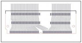
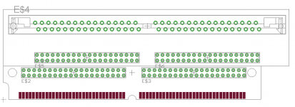
I think it's been said earlier, but I would consider doing the design in Eagle CAD and fabbing it at Seed Studio. Part of the proof of concept should include connectors that you would use in the real end product. It would also be much easier to build, just solder in the connectors and plug them in with cables. Eagle is a little clunky... I made this example using their standard libraries, I would make the spacing between the two halves a little different for room for cutting (and remove the cut line in the middle), but this was a quickie. Your Illustrator skills would help with routing the lines.

extender concept.png

 
Top