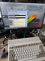
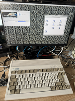
New Project: DoubleVision SE/30 Card

Hello Mac community,

since I have gotten my first actual Macintosh last month (LC475), I must admit that the "Mac Bug" has bitten me, which is why I have now also pushed the trigger on getting a Macintosh SE/30 yesterday.

In order to have fun with it, I decided to port one of my other Amiga projects to the SE/30, therefore, I would like to announce today that I have started to develop a new graphics card for the SE/30 called:

DoubleVision SE/30

Technically, it is very much a Macintosh port of my Amiga graphics card, the P-Vision, but with some Mac SE/30 specific feature enhancements. ;)

So what can it do? Well, here is the feature List:

  • HDMI video plug using DVI video signalling
  • 32MB VRAM framebuffer, clocked at 165MHz
  • Supports 1bit,2bit,4-bit,8bit,15bit,16,bit and 32bit color depths
  • All standard VGA and MAC resolutions, supporting up to 1280x1024@60p AND 1920x1080@30p
  • Fast 64-bit BitBlt engine, pushing up to 130 Mio Pix/s (8bpp)
  • 32 KB internal ROM for graphics drivers
  • Firmware can be fully upgraded on the host system (via "FlashFPGA App" running on MacOS)
  • Special MAC SE/30 features:
    • Card can work in dual-mode (second monitor to the SE/30 internal monitor) or route the SE/30 internal video output to HDMI
    • If MAC is booted, and no HDMI is connected, framebuffer memory is added as 32 MB system memory
    • Eleborate write-through cache to minimise read/write latency to VRAM
    • Makes full use of 68030 2-cycle 32-bit synchronous bus termination - yielding up to 32MB/s host memory performance using 16MHz bus!
I have seen that MAC SE/30 graphics cards using old and outdated graphics chips fetch high prices on the collector's market, so here is my offer to the community to provide a much more modern and better solution.

The card itself is low-profile and it has an internal HDMI port, which can be put outside of the SE/30 via a small bracket.

As I said, most of the development is already done, as the designs works great on the Amiga, therefore I expect that the most challenging part for me is to write the graphics ROM driver for the MAC in order to enable the display output. I have already started to look into this direction. ;-)

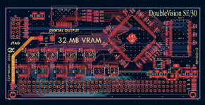
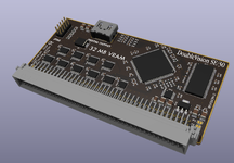
So for now, let's start with a first render of the board PCB, which I expect will be nearly identical to the final PCB.
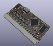
Screenshot 2026-01-19 092730.png

As always, questions, comments, etc are always welcome. :)
 
Dedicated chip(s) for video and/or acceleration, or are you using a FPGA for everything ? The rendering show quite a small chips for a FPGA (... but then I went a bit overkill :-) I could probably get two Full HD output if I really wanted to... ).

@zigzagjoe has a SE.30 video board with a dedicated chip, the 30Color.

My IIsiFPGA is targeted at the IIsi; should work in a SE/30 but it might not physically fit. You can find the source code for the DeclROM in the VintageBusFPGA repository on GitHub. So is the firmware for the custom VexRISCV core used for acceleration. The acceleration INIT and the audio driver (when using the PHY with 'true' HDMI signalling, instead of the DVI-like PHY - though this last one supports many hardware resolution via PLL reconfiguring while the 'true' one is just one hardware resolution + windowbonxing) is in the NuBusFPGA repo. Maybe it can help getting you started with the software (... mine is GPL BTW).

Acceleration is the PITA part. You need to hack into QuickDraw in a very ad-hoc fashion, peeking and poking in memory... it's not pretty. That's why I only did blitting, when the hardware could theoretically do all of it (it's just a CPU and some C code!), same as the 8*24GC board did.

Edit: forgot to say, there's also a Rom patch for the IIsi to add an extra memory bank to use the FPGA spare memory as extra RAM. Testing an additional 240 MiB of RAM at boot takes a loooooong time.
 
Last edited:
If only this would be also compatible with IIsi and A/UX ... 😇

If the driver is well-behaved it ought to be, at least under A/UX 3. A/UX 3 runs the mac display driver in a kind of demented cradle, lying to it frantically to try to stop it realising it's not running under MacOS. Note though that this is not the same demented cradle that other bits of Mac software run in (that's demented in a rather different way) so things like anything patched in an INIT won't work. The driver will have to be self-contained, as it should be.
 
Dedicated chip(s) for video and/or acceleration, or are you using a FPGA for everything ? The rendering show quite a small chips for a FPGA (... but then I went a bit overkill :-) I could probably get two Full HD output if I really wanted to... ).

@zigzagjoe has a SE.30 video board with a dedicated chip, the 30Color.

As with all my projects, they are FPGA based. Inside the FPGA, I'm using a full 64-bit datapath for everything, and a highly pipelined memory transaction arbiter, controller, display engine and BitBlt engine.

Even without using the BitBlt engine, at least on Amiga, the design is fully usable even using an 68EC020 CPU at 14.3MHz using 8-bit color depth at 1920x1080. I expect that at least the same can be achieved on a stock SE/30, or even better using the full 32-bit synchronous data path.

My IIsiFPGA is targeted at the IIsi; should work in a SE/30 but it might not physically fit. You can find the source code for the DeclROM in the VintageBusFPGA repository on GitHub. So is the firmware for the custom VexRISCV core used for acceleration. The acceleration INIT and the audio driver (when using the PHY with 'true' HDMI signalling, instead of the DVI-like PHY - though this last one supports many hardware resolution via PLL reconfiguring while the 'true' one is just one hardware resolution + windowbonxing) is in the NuBusFPGA repo. Maybe it can help getting you started with the software (... mine is GPL BTW).

Wow, thanks a lot! :) I have started to read the "Designing Cards and Drivers for the Macintosh Family" guide, and have seen that there is actually exaple code for a skeleton graphics driver present there.

Acceleration is the PITA part. You need to hack into QuickDraw in a very ad-hoc fashion, peeking and poking in memory... it's not pretty. That's why I only did blitting, when the hardware could theoretically do all of it (it's just a CPU and some C code!), same as the 8*24GC board did.

It's actually very much the same on the Amiga as well. The OS provides hardware acceleration functions for the Amiga Blitter in the "graphics.library", but no interfaces to defer the functions to a different rendering target. That's why, in the 90's, several frameworks were developed to add this missing layer, which Commodore did not get around to implement. And it works really well!

Edit: forgot to say, there's also a Rom patch for the IIsi to add an extra memory bank to use the FPGA spare memory as extra RAM. Testing an additional 240 MiB of RAM at boot takes a loooooong time.

I can imagine, luckily, my card provides only 32MB of VRAM. ;)

Thanks for your help!
 
As with all my projects, they are FPGA based
Hehe, me too. Much more fun to be able to fix/update/improve/extend the design even after the hardware is done :-)

.Inside the FPGA, I'm using a full 64-bit datapath for everything, and a highly pipelined memory transaction arbiter, controller, display engine and BitBlt engine.
Neat. Is it purely for your own stuff or di you open-source it ?
My design is less efficient - it's essentially a CPU-less soft-SoC using Litex, with a bridge from the original bus (SBus originally, then NuBus, '030 and '040). Main bus is just a 100 MHz Wishbone, and the peripherals are mostly from Litex (e.g. the memory controller is LiteDram). I hadn't done any hardware before the original SBusFPGA, Litex was the reason I was able to do some "sophisticated" stuff.
The original accelerator was going through the Wishbone, but I eventually implemented a dedicated 128-bit bus from the VexRISCV D-cache to the LiteDram arbiter. Probably overkill - i meant to try NaxRISCV as the accelerator, but last time I looked it was still a bit too feature-rich (my version of the VexRISCV is really just a glorified micro-controller with some custom instructions to better support X11 acceleration including XRender and unaligned blitting in QuickDraw).

Even without using the BitBlt engine, at least on Amiga, the design is fully usable even using an 68EC020 CPU at 14.3MHz using 8-bit color depth at 1920x1080. I expect that at least the same can be achieved on a stock SE/30, or even better using the full 32-bit synchronous data path.
1920x1080 is OK on '030 in 8-bits or less on e.g. a IIsi, or anything with a NuBus slot (which is the bottleneck), but not fast. 32-bits is too slow without acceleration, and even with acceleration it's not super comfortable (I should so more acceleration...). It's much better on the QuadraFPGA where the FPGA connects directly to the '040 bus - BW and latency are almost good enough, and with acceleration it's usable even in 32-bits. Also fine on SBus using EXA/XRender on my SPARCstation 20 (on my incredibly large back-burner, there is supporting USB and accelerated X11 in NetBSD/mac68k...).

Though truth be told, unless doing vintage Photoshop, there's not mych reason for 32-bits on vintage Macs. If I had the skill for the PCB, I'd have a go at a much cheaper version with a Spartan-7 (instead of the Artix-7) with 1024x768/32, 1280x1024/16 and 1920x1080/8 as the targets. But designing the DDR[23] interface is too complex, and Spartan-7 aren't really designed to support single-sided (read: assembled for cheap by JLCPCB!) board with their decoupling requirements :-( But then I guess it's no longer a problem as you're about to fill that niche anyway :-)

Wow, thanks a lot! :) I have started to read the "Designing Cards and Drivers for the Macintosh Family" guide, and have seen that there is actually exaple code for a skeleton graphics driver present there.
The example code is ... a starting point :-/ I had a lot of trial-and-error to figure out how everything worked in various OSes, and the godsend for me was QEmu. I just hacked a version of QEmu with could emulate a Q800 to create a model of my (unaccelerated) device, and developed the ROM on that. It helped a *lot*.

It's actually very much the same on the Amiga as well. The OS provides hardware acceleration functions for the Amiga Blitter in the "graphics.library", but no interfaces to defer the functions to a different rendering target
Even if not perfect, that sounds a bit more comfortable than the horror that is QuickDraw acceleration :-/ There's no provision for acceleration at all up to at least MacOS 8, and the functions you can substitute for (by gijacking the traps...) are quite high-level. I highly recommend sorting out all the dumb framebuffer stuff before even thinking about acceleration... it's a really deep rabbit hole to get into.
 
Hehe, me too. Much more fun to be able to fix/update/improve/extend the design even after the hardware is done :-)

Definetely, and it's also my preferred modus operandi, since I come from the semiconductor industry. So for me, FPGA is real hardware. ;)

Neat. Is it purely for your own stuff or di you open-source it ?

I'm considering to open source it - at least the PCB files and software. I'm doing this for fun, not for any commercial "gains" (which is impossible, given the amount of unpaid engineering hours being spent on such projects).

My design is less efficient - it's essentially a CPU-less soft-SoC using Litex, with a bridge from the original bus (SBus originally, then NuBus, '030 and '040). Main bus is just a 100 MHz Wishbone, and the peripherals are mostly from Litex (e.g. the memory controller is LiteDram). I hadn't done any hardware before the original SBusFPGA, Litex was the reason I was able to do some "sophisticated" stuff.

Which is completely okay. You do this for fun, possibly to gain new skills and experiences, and it's often better to get anything out first, rather than waste time on perfectionism. Due to my experiences, I usually have a good feeling about what resources are needed for a specific design. In this case, I'm using an FPGA with 8-16K LEs, depending on if I can make the blitter work reasonably well in a Mac environment. On Amiga, it works really well.

The original accelerator was going through the Wishbone, but I eventually implemented a dedicated 128-bit bus from the VexRISCV D-cache to the LiteDram arbiter. Probably overkill - i meant to try NaxRISCV as the accelerator, but last time I looked it was still a bit too feature-rich (my version of the VexRISCV is really just a glorified micro-controller with some custom instructions to better support X11 acceleration including XRender and unaligned blitting in QuickDraw).

Going RISC-V would also be my choice if I wanted to have a more flexible design. The blitter itself is actually quite close to a typical 90's bit blitting engine you would find in such designs from ATI, S3 or Cirrus Logic.

1920x1080 is OK on '030 in 8-bits or less on e.g. a IIsi, or anything with a NuBus slot (which is the bottleneck), but not fast. 32-bits is too slow without acceleration, and even with acceleration it's not super comfortable (I should so more acceleration...).

32-bit becomes usable starting with a 50MHz 68030. On the Amiga, the bottleneck of my card is actually the PCMCIA bus, which maxes out at 8.5 MB/s. But since, on the SE/30, the full 32-bit synchronous bus is exposed, I really think this will work much better. Then it's mostly a matter of how well QuickDraw if optmizised for software rendering - which I believe might be superior to the software renderer mode of the Amiga graphics card framework.

It's much better on the QuadraFPGA where the FPGA connects directly to the '040 bus - BW and latency are almost good enough, and with acceleration it's usable even in 32-bits. Also fine on SBus using EXA/XRender on my SPARCstation 20 (on my incredibly large back-burner, there is supporting USB and accelerated X11 in NetBSD/mac68k...).

Hehe, you seem to be quite a busy and passionate individual! :) I'm glad that I joined this Forum, quite interesting things going on here.

Though truth be told, unless doing vintage Photoshop, there's not mych reason for 32-bits on vintage Macs. If I had the skill for the PCB, I'd have a go at a much cheaper version with a Spartan-7 (instead of the Artix-7) with 1024x768/32, 1280x1024/16 and 1920x1080/8 as the targets. But designing the DDR[23] interface is too complex, and Spartan-7 aren't really designed to support single-sided (read: assembled for cheap by JLCPCB!) board with their decoupling requirements :-( But then I guess it's no longer a problem as you're about to fill that niche anyway :-)

My attempt is to max-out a relatively constrained design, so I pay very much attention to things like memory arbitration, and designing the memory controller in a way to provide the right transaction scheduling strategy to max out the DRAM interface. Doing this, you will be surprised how much can be achieved using only a 16-bit SDR SDRAM chip. I'm also trying to keep it "solderable" so that people can manufacture their own cards.

The example code is ... a starting point :-/ I had a lot of trial-and-error to figure out how everything worked in various OSes, and the godsend for me was QEmu. I just hacked a version of QEmu with could emulate a Q800 to create a model of my (unaccelerated) device, and developed the ROM on that. It helped a *lot*.

Again, thanks a lot for offering your valuable work. As I said, once I am finished, I'm actually going to open source this design as well.

Even if not perfect, that sounds a bit more comfortable than the horror that is QuickDraw acceleration :-/ There's no provision for acceleration at all up to at least MacOS 8, and the functions you can substitute for (by gijacking the traps...) are quite high-level. I highly recommend sorting out all the dumb framebuffer stuff before even thinking about acceleration... it's a really deep rabbit hole to get into.

Sure, the blitter is just part of the design, because it's already existing from the Amiga use-case.
 
Definetely, and it's also my preferred modus operandi, since I come from the semiconductor industry. So for me, FPGA is real hardware. ;)
Yes, FPGA feels a lot more like hardware than software emulation. And things like PiStorm and other feel a bit off to me - when going SW, might as well go into it fully like QEmu or MAME.

I am in the semiconductor industry as well, on the design side - waiting for a chip back from TSMC at the moment - which I joined a couple of weeks after the Covid lockdown started in France back in 2020. At that point, locked at home and needing to understand the vocabulary of my true hardware colleagues (so many words that seem to mean the same things than to SW people but not really...), the SBusFPGA started with just the hope of blinking a Led someday :-) But I never encountered a rabbit hole I didn't want to explore and map fully... and I think I'm still the only person in the world to have USB and HDMI on a SPARCstation :-)

BTW, have you looked at the open PDKs and open-source EDA stuff ? Nowhere near the level of leading-edge, but the SKY130 should be able to produce some interesting replica/update of 80s and 90s chips...

Due to my experiences, I usually have a good feeling about what resources are needed for a specific design
Hehe, due to my lack of experiences, I just over-engineer everything - or at least I think I do! :-)

Though I'm not the worst - I use an Artix-7 35T in the *FPGA, and I have considered projects with 100T. I know of a (non-pubic) project of another FPGA-based video board for the SE/30, and they used a Kintex-7 325T... that FPGA will host quite a bit of hardware! (... if you have the license for Vivado).

Going RISC-V would also be my choice if I wanted to have a more flexible design. The blitter itself is actually quite close to a typical 90's bit blitting engine you would find in such designs from ATI, S3 or Cirrus Logic.
I tried to design one, but misaligned accesses was a bit much and I couldn't figure it out (based on, of all things, a crypto engine...). That's when I switched to a simple CPU core. It's also more versatile ; XRender tends to use funky arithmetic to implement acceleration - it has a datatype over 8 bits that represent [0-1.0], so (255*255) is supposed to output 255... So I added an instruction to do four (a*b)/255 in a 32-bits register used as 4*8-bits (SIMD). I also added double-register (64-bits) load/store to improve bandwidth a bit. But it's probably not very area-efficient for its purpose.

Then it's mostly a matter of how well QuickDraw if optmizised for software rendering - which I believe might be superior to the software renderer mode of the Amiga graphics card framework.
Well, I don't know anything on the Amiga side, but while the B&W QD code on the 68000 was very efficient, I'm not so sure about all the extra stuff they added in Color QuickDraw... and it's a complete mess as an implementation, when judged by modern standard.

My attempt is to max-out a relatively constrained design
I come from a HPC background; we do optimize software (and a lot of it is still Fortran, so no tmany yuoungsters going into it ;-) ), but otherwise we just throw hardware at the problem :-) The only people that are worse (way worse) than us are the AI people. We still count in thousands of CPU cores; they moved on to counting megawatts and gigawatts directly...

so I pay very much attention to things like memory arbitration, and designing the memory controller in a way to provide the right transaction scheduling strategy to max out the DRAM interface. Doing this, you will be surprised how much can be achieved using only a 16-bit SDR SDRAM chip.
Makes me think of a question: you connect the SDRAM to the CPU bus directly and use the FPGA as a memory controller? [which would explaing getting away with just a QFN?] Or is the CPU <=> memory path going through the FPGA? I use the second option (so all the hard PCB stuff is on a FPGA board I just buy), but readback latency sucks. It also burns pins on the FPGA to support the parallel busses, requiring a big FPGA board and limiting the number of peripherals you can add on the FPGA (if you have a biggish FPGA, might as well make the board multi-functions!).

I know SDRAM can be used on those vintage CPU (there's a SDRAM board for the SE/30 on this very forum, and before that I saw some Amiga accelerators and homebrews also using SDRAM), but I never finished my attempt at implementing it. The timing trickery to get the appropriate setup/hold time from the SDRAM is still beyond me.

I'm also trying to keep it "solderable" so that people can manufacture their own cards.
Never been good at it, terrible eyesight that keeps getting worse => JLCPCB (and before that, SeeedStudio) is my lifesaver. I still can do 2.54mm pitch through-hole, and I did 1.27mm by taking the time not too long ago (SBus connector). JLCPCB does 0402s for dirt cheap, so usually I just pay them to do it for me...
 
I am in the semiconductor industry as well, on the design side - waiting for a chip back from TSMC at the moment - which I joined a couple of weeks after the Covid lockdown started in France back in 2020. At that point, locked at home and needing to understand the vocabulary of my true hardware colleagues (so many words that seem to mean the same things than to SW people but not really...), the SBusFPGA started with just the hope of blinking a Led someday :-) But I never encountered a rabbit hole I didn't want to explore and map fully... and I think I'm still the only person in the world to have USB and HDMI on a SPARCstation :-)

It's quite a challenge to acquire new skills, especially when you are basically working in an isolated environment without getting to meet your colleagues F2F. Has been quite a challenge for me as well, but in the meantime, I have gotten used to it.

BTW, have you looked at the open PDKs and open-source EDA stuff ? Nowhere near the level of leading-edge, but the SKY130 should be able to produce some interesting replica/update of 80s and 90s chips...

It's then "only" a matter of producing this ASIC. ;)

Hehe, due to my lack of experiences, I just over-engineer everything - or at least I think I do! :-)

Though I'm not the worst - I use an Artix-7 35T in the *FPGA, and I have considered projects with 100T. I know of a (non-pubic) project of another FPGA-based video board for the SE/30, and they used a Kintex-7 325T... that FPGA will host quite a bit of hardware! (... if you have the license for Vivado).

Yeah, same stuff happened on the Amiga as well, and my answer to that was the P-Vision, showing I can basically do the same things on a $30 FPGA in TQFP package. ;-) I guess that's why I am also attached to retro designs, because it remebers us that basically most of the work can be accomplished with a lot less resources.

And it's also a good education for my kids, who will have the benefit of still learning how computers REALLY do work.

I tried to design one, but misaligned accesses was a bit much and I couldn't figure it out (based on, of all things, a crypto engine...). That's when I switched to asimple CPU core. It's also more versatile ; XRender tends to use funky arithmetic to implement acceleration - it has a datatype over 8 bits that represent [0-1.0], so (255*255) is supposed to output 255... So I added an instruction to do four (a*b)/255 in a 32-bits register used as 4*8-bits (SIMD). I also added double-register (64-bits) load/store to improve bandwidth a bit. But it's probably not very area-efficient for its purpose.

If it gets the job done, why complain. ;-) Your next attempt will benefit from having it already done by yourself.

Makes me think of a question: you connect the SDRAM to the CPU bus directly and use the FPGA as a memory controller? [which would explaing getting away with just a QFN?] Or is the CPU <=> memory path going through the FPGA? I use the second option (so all the hard PCB stuff is on a FPGA board I just buy), but readback latency sucks. It also burns pins on the FPGA to support the parallel busses, requiring a big FPGA board and limiting the number of peripherals you can add on the FPGA (if you have a biggish FPGA, might as well make the board multi-functions!).

Very simple, SDRAM is connected to FPGA, and the whole address / data bus of the 68030 is multiplexed (hence the sh*tload of bus drivers on the PCB). This basically yields the same performance as using a non-multiplexed bus, AND, I have full access to all data and adressbits of the CPU. Meaning, I can implement an efficient write-buffer strategy to sustain, at least, the maximum write performance to VRAM.

For reads, I'm planning to use the block ram to implement a small L2 cache.

I know SDRAM can be used on those vintage CPU (there's a SDRAM board for the SE/30 on this very forum, and before that I saw some Amiga accelerators and homebrews also using SDRAM), but I never finished my attempt at implementing it. The timing trickery to get the appropriate setup/hold time from the SDRAM is still beyond me.

Well, SDR SDRAM is way more forgiving in this regard than DDR2/3/4/5 designs. ;-) On P-Vision, I can reach 165MHz memory bus without a sweat. You have, of course, to pay attention to timing constraining your design reasonably well (my memory controller can even run at 190Mhz - so there is still enough breathing room.)

Never been good at it, terrible eyesight that keeps getting worse => JLCPCB (and before that, SeeedStudio) is my lifesaver. I still can do 2.54mm pitch through-hole, and I did 1.27mm by taking the time not too long ago (SBus connector). JLCPCB does 0402s for dirt cheap, so usually I just pay them to do it for me...

Funny you mention this, because today, I picked up my new glasses. :)
 
Back
Top