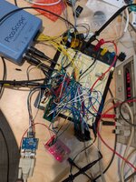
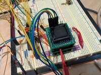
My understanding of the IWM spec (and the Disk II) continues to evolve, albeit slowly.
In the Disk II, Q3 (2 MHz, twice the clock frequency of the Apple II) is the only clock that exists, so it's used for everything. In the IWM, Q3 is only used for writing data in synchronous mode, FCLK (in fast mode, FCLK/2 in slow mode) is used for everything else. That makes sense, you'd kind of want to use the fastest clock you have in order to have the highest resolution available for clock recovery.
What's still stumping me is "port operation":
I would sort of like to know whether this mode was actually used anywhere or whether this was merely a theoretical use case that the IWM supported. More than that, though, I'd like to understand exactly how one was supposed to use it. On a superficial level it makes sense, you're basically using the IWM as a serial-in-parallel-out shift register where the input is asynchronous. But in order to set it up this way, you'd need to write the mode register at least once, which would require flipping the L6 and L7 soft switches and writing the data bus, so the address and data lines would have to be connected to the processor - whose data bus would then be monopolized by the IWM when you hold !DEV low. This makes no kind of sense to me. I'd love to ignore it, but Apple clearly thought it was important enough to include in the spec, and I'm worried that understanding what's going on will be important in order to be able to mimic the behavior of the chip.
In the Disk II, Q3 (2 MHz, twice the clock frequency of the Apple II) is the only clock that exists, so it's used for everything. In the IWM, Q3 is only used for writing data in synchronous mode, FCLK (in fast mode, FCLK/2 in slow mode) is used for everything else. That makes sense, you'd kind of want to use the fastest clock you have in order to have the highest resolution available for clock recovery.
What's still stumping me is "port operation":
In port operation, which is asynchronous mode true and latch mode false with /DEV held low indefinitely, read data will appear and change as if the IWM were being continually read. In port operation the MSB can be used to continuously clock data into external registers. The MSB will be cleared at least six FCLK periods before being set. Except in port operation, in asynchronous mode the latch mode bit should be set (for reliability in clearing the data register after a read).
I would sort of like to know whether this mode was actually used anywhere or whether this was merely a theoretical use case that the IWM supported. More than that, though, I'd like to understand exactly how one was supposed to use it. On a superficial level it makes sense, you're basically using the IWM as a serial-in-parallel-out shift register where the input is asynchronous. But in order to set it up this way, you'd need to write the mode register at least once, which would require flipping the L6 and L7 soft switches and writing the data bus, so the address and data lines would have to be connected to the processor - whose data bus would then be monopolized by the IWM when you hold !DEV low. This makes no kind of sense to me. I'd love to ignore it, but Apple clearly thought it was important enough to include in the spec, and I'm worried that understanding what's going on will be important in order to be able to mimic the behavior of the chip.


