Testing a 6200 and comparison with 6100

( @Phipli ) it adds up, but there are a few reasons why I don't think that's the cause.

Firstly, there are no Read-Modify-Write memory instructions on a PowerPC, just load and store. So, this sequence of bus cycles in non-cached DRAM would have to be implemented in software, not the Capella bridge chip (load a 32-bit word to a register; insert the byte into the right position; write the long word back). But that doesn't make sense either, it would mean that the ROM had to consider the underlying PPC/'040 bridge.

Secondly, I don't think it makes sense to be implemented in Capella either. For cachable addresses, whole words get loaded into L2, then L1 cache - a block of 32 bytes (8 words) are loaded at a time and if a byte or half-word is modified there (which is now on the PPC side of course), the whole word (i.e. 8 words) would be written when the cache line needs to be flushed. So cacheable memory never needs an RMW sequence, nor a byte modification sequence.

Thirdly, from the developer note, it seems fairly clear that the interface between the 68040 bus to the PPC603 is a set of 543 latches:


So, I don't think it makes sense for Capella to emulate a byte store to uncached RAM to load an entire word into the D-latches from DRAM, then modify the intended byte, then write the 32-bit word back out. For byte loads it wouldn't matter, a PPC603 would still just load a 64-bit double-word and select the right byte.

It also makes little sense, given that the only way Capella can know if there's a non-cacheable byte write is if the PPC603 tells it. So, there are signals from the CPU for that purpose. It's far easier for DRAM to include byte line selects and simply pass those signals on. Even though the CPU will probably send out 64-bits + the byte select signals; Capella must know how to select the high or low 32-bit word, because DRAM is 32-bits wide. It must do that for normal writes anyway.


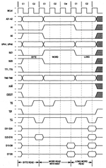
From page 8-15 it works like this:

A29-A31 (which are the low-order bits in the insane IBM convention), select the byte lane while the 3 signals TSIZ0:2 ==001, meaning 1 byte.

It's very easy for Capella to use this information to select the right byte lane in DRAM. A similar approach works for 16-bit and 32-bit read/writes:

Poor Video RAM performance is, I would deduce, for other reasons.
Sorry, I think you are confused or missing my point, perhaps I was unclear.

I don't mean a read-modify-write sequence as in an instruction that causes a read-modify-write bus cycle. I don't think the 68K ROM used these as only specific instructions use them. I'm referring to the QuickDraw use case of reading a particular address (framebuffer for a particular pixel), modifying the data, then writing it back. The point of mentioning byte width (as an example for 8bpp) is that an entire bus transfer cycle is required regardless of width if the address is cache inhibited. If for each pixel changed you're doing two full bus cycles, as I said, that gets expensive quickly because you accumulate additional wasted cycles from bus translation overhead.

Edit: To further clarify, most QuickDraw accesses act like that - basic drawing instructions and the like. In some cases it's possible to do larger transfers (blits, moves, and the like) but that depends a lot on the specific request, organization of framebuffer memory, bit depth, etc. A line from A to B is going in most cases to cause a series of single-pixel changes requiring that exact read-modify-write trace (but not a RMW cycle) I mentioned above as the framebuffer is typically cache inhibited.

Cache inhibition can be a handled a couple of two ways. Most commonly it's handled by MMU flags on particular pages/portions of address space that indicate if the caches should be inhibited or not. This is how apple did it on all models of 68K mac and I would assume on PPC as well. It's possible for an external device (at least on 040) to indicate that a particular transfer shouldn't be cached, but this should only be used in very specific cases. Assuming the page is marked as cache inhibited via the MMU, on any access, the caches will not be checked nor will the result of the bus cycle be stored in cache. On an 040 this is the primary way a bus cycle of less than a line width would happen.

You want to inhibit the caches for IO devices, for example, and other circumstances where the contents of the addressed memory may change unexpectedly (DMA). In most 68K macs only the ROM and (most) main memory DRAM is cachable; nubus space and IO space is not and framebuffer lives somewhere in there.
 
Last edited:
<snip> perhaps I was unclear. <snip> I'm referring to the QuickDraw use case of reading a particular address (framebuffer for a particular pixel), modifying the data, then writing it back. <snip> bus translation overhead <snip> most QuickDraw accesses act like that - basic drawing instructions and the like. In some cases it's possible to do larger transfers (blits, moves, and the like) but that depends a lot on the specific request, organization of framebuffer memory, bit depth, etc. A line from A to B is going in most cases to cause a series of single-pixel changes requiring that exact read-modify-write trace (but not a RMW cycle) I mentioned above as the framebuffer is typically cache inhibited.


Cache inhibition <snip> MMU flags on particular pages/portions of address space <snip> main memory DRAM is cachable; nubus space and IO space is not and framebuffer lives somewhere in there.
Indeed. So, on a 6100, video is in DRAM. So, that means that area of DRAM gets marked as non-cacheable. On a 6200, the frame buffer is 1MB of DRAM behind Valkyrie, which can store up to 4x transactions.

So, to properly resolve the question I think someone needs to write a couple of tests to work out what the cost of the bus translation overhead is. Reading other similar threads, to which we've contributed:


Then people like @Melkhior seem to know how the 603 to '040 bus interface worked and somewhere in my hazy memory I recall seeing a diagram, but I've no idea where. Finally, one of the comments on these threads claimed the '040 bus worked at 37.5MHz, not 33MHz. Surely the mismatch would cause a pretty bad overhead in most circumstances & not just graphics, not least because a P5200's 32-bit '040 data bus is half the width of the 6100's: 68K emulation would be badly affected too. Finally, @noglin estimated that although writes to Valkyrie were fast, reads could take ≈50 x PPC 603 cycles.

And one other thing, the Dev note says Valkyrie's clock is synced to the CPU clock for performance reasons during data transfers. So, given that it's on the '040 side; it seems to me that the '040 bus also runs at 37.5MHz, because otherwise you'd get extra cycles inserted for the bus interface and on top of that Valkyrie would have to sync to the PPC603, which surely would slow things down even further?

Perhaps there's another possibility, not related to the '040 bus itself, nor QuickDraw, but maybe the TLB? The 603 has an inverted page table, but TLB misses are handled in software via an interrupt. I understand that Inverted page tables were so awful, Apple didn't use the standard 8-cycle TLB miss interrupt, but their solution, though faster (or better) than Inverted Page Tables was still much slower than 8-cycles.

If so, we may have a rationale for why QuickDraw is slow on a P6200/P5200 vs a Q630 vs a PM6100:

  1. Both the Q630 and PM6100 have hardware TLB walks, so these will be fast.
  2. Some QuickDraw operations could quite easily hammer the TLB in a way that general 68K emulation doesn't, because they're far more non-local. e.g. when you draw a vertical line you're skipping 640b at a time at 640x480x8bpp; that's 1x 4K page fault every 6.4 pixels.
  3. OTOH 68K code has a high degree of locality.
  4. Therefore, the P5200/6200 graphics are a pathological case.
I freely admit I might be talking tosh here, but at least I have a claim to some imaginative tosh 😁 Now it's midnight and my brain is fried. Serves me right ;) !
 
Anecdotally, I used a Performa 6200 as my main machine for about 3 years or so, and I have owned several since. I never really noticed a speed problem, because my machine before the 6200 was an SE. I also had use of a 4400 around that time, but the 6200 always performed fine at what I used it for: ClarisWorks, Warcraft II, Photoshop, REALBasic. I even used to render images with Bryce 2 on it, it took an age but it was worth the wait, I wish I still had those Bryce files from back then. People have to remember what the machines were intended for and what else was around at the time. Macs were hellishly expensive, a lot of people would've still been using Pluses/SEs around the time the 6200 was released. It was a huge jump from those machines.
 
Anecdotally, I used a Performa 6200 as my main machine for about 3 years or so, and I have owned several since. I never really noticed a speed problem, because my machine before the 6200 was an SE. I also had use of a 4400 around that time, but the 6200 always performed fine at what I used it for: ClarisWorks, Warcraft II, Photoshop, REALBasic. I even used to render images with Bryce 2 on it, it took an age but it was worth the wait, I wish I still had those Bryce files from back then. People have to remember what the machines were intended for and what else was around at the time. Macs were hellishly expensive, a lot of people would've still been using Pluses/SEs around the time the 6200 was released. It was a huge jump from those machines.
Yeah, there is nothing wrong with it.

The discussion around the video performance is driven by wondering can we improve it given it is lower than expected. Otherwise, I don't feel that previous claims about 68k emulation performance and L1 cache limitations actually bear fruit.

I suspect in part people just didn't understand that 75MHz doesn't always mean faster than 66MHz.
 
Yeah, there is nothing wrong with it.
Yes, and case in point: my dad ran his graphic design business on a 6200 for ~4 years. It certainly wasn't the ideal machine for that job, but it got him by until he upgraded to a G4. Power Macs before the G3s came out were silly price, so for a one man band operation the Performas were much more acheiveable.
 
Yes, and case in point: my dad ran his graphic design business on a 6200 for ~4 years. It certainly wasn't the ideal machine for that job, but it got him by until he upgraded to a G4. Power Macs before the G3s came out were silly price, so for a one man band operation the Performas were much more acheiveable.
Exactly this. I couldn't afford a IIci when I was in college and starting my own studio, all I could afford was a IIsi. I did what I could with what I had — it wasn't my dream setup but it was still good enough.
 
Nice article!

I'd love to compare a release day ROM to see if graphics performance is better.

I have a 6200 that was recently “repatriated” last year that I’d given to my sister ~25 years ago for web design. As a primarily Windows-based user, she needed to be able to see how her pages looked on a Mac. It certainly performed sufficiently for that task, at the time.

I do not remember what ROM it has, but I will check.
 
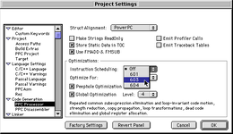
@Phipli : I checked the compiler options for my Code Warrior Gold 11 (Academic) to see how they differ from yours. And indeed there are fewer options:

CWGold11PpcOpts.png
As you can see, only the PPC601, 603 and 604 were supported at the time (I picked it up in late 1996), not the 603e, 604e and 750.

Yeah, there is nothing wrong with it.
This is one of the reasons why I keep hoping there's going to be an InfiniteMac.org P5200 emulator at some point. DingusPPC can emulate a PPC603, but Valkyrie isn't emulated yet. Still, I think enough is understood about the chip to implement pretty much every use of it. Also it'd mean the Q630 could be added.
The discussion around the video performance is driven by wondering can we improve it given it is lower than expected. Otherwise, I don't feel that previous claims about 68k emulation performance and L1 cache limitations actually bear fruit.
Which is why I think the first step is to figure out what causes the slowdown in current tests.
I suspect in part people just didn't understand that 75MHz doesn't always mean faster than 66MHz.
Possibly. I decided to see if I could find a review of the P5200 online. MacWorld has one (on Archive.org), and there's a section on performance which is instructive:

1770722422305.png
If this was true, it means the '040 bus runs at 3 PPC cycles per '040 bus cycle and this would explain quite a bit of the performance hit. How could we prove this? I'm not sure how to force regions of RAM to be uncacheable, but I don't think we need to as we can make use of what we understand from the L1 (writeback, 2-way) and L2 (writethrough) caches with 32-byte cache lines each. Consider these PPC tests:

  • Take a single L1 data cache line, which can be generated by allocating 64 bytes of RAM and constructing a pointer aligned to 32-bytes. Write 32-bytes of data repeatedly to the same cache line (millions of times), incrementing 32-bit values will do, we need to write 8 of them per pass. This measures the L1 bandwidth for one way, it's a write-back cache so it doesn't go out to L2. The test loop needs to otherwise use only registers (we have 32 so that should be OK).
  • A similar test follows: allocate a 4kB+64b block of RAM; generate 2 pointers at the base address+whatever to align to 32 bytes; then that base address + 4kB. This accesses both sets. Write the same sets of data to both lines alternately. This measures the L1 bandwidth for both sets. The result should be the same bandwidth.
  • The third test extends this a little further, we generate a 12kB+64b block of RAM and generate 4 pointers: int32_t *p0=((baseAddr+31)&~32), *p1=&p0[1024], *p2=&p1[1024], *p3=&p2[1024]; This time when we write to p2 and p3 it will force an L1 cache line flush into L2, and then the same thing will happen when we write back to p0 and p1. But because L2 is write-through, it will force an L2 cache line flush too, writing to the '040 bus. Since the CPU <--> L2 bus is 64-bits (8B), there are 8 writes at a time. The CPU will write the first long word, I think, in 2 x 37.5MHz cycles, and would like to write the rest in 1 cycle each. However, because the L2 cache is write-through and this behaviour is governed by Capella, all those writes will go immediately to the '040 bus as well; which means the first write will take 2x37.5MHz cycles (because it'll go into the latches), but the rest will take much longer: approximately 4x37.5MHz cycles per word if the '040 bus runs at 33MHz or 6x37.5MHz if it runs at 25MHz (3 cycles per 32-bit word x 2 words per 64-bit word). But ultimately, the speed might be limited by the DRAM, which I think is 80ns (12.5MHz for a /RAS + /CAS or 25MHz for other words in the page).
  • The fourth test is like the third, but the pointer is set to somewhere in the VRAM address space (which is listed in the developer note). This tests whether VRAM performs higher than DRAM even though it's uncacheable. My understanding is that it is, because it's 60ns DRAM.
We can then repeat the set of scenarios with a slightly different test. In this case instead of writing an updated counter from a register, we read from the pointer; add a value and write it back. L1 performance should be very high. L1+L2 tests should now be faster than the one where we hit video RAM, because although L1 gets flushed and L2 is write-through, reads will read from the L2 cache, because that's 256kB. The final test essentially tests @zigzagjoe 's hypothesis, I think. My guess is that the final test will be dramatically slower, because Valkyrie prioritises writes over reads!

If so it'd tell us how to improve performance a little. If DRAM reads are fairly fast, then we could in theory, cache video in DRAM, essentially as an off-screen pixmap. RMW graphics go to that fake buffer, but later are pushed to Valkyrie. We can also use that mechanism to independently test the actual performance of QuickDraw by writing our test routines to go to only off-screen pixmap instead of on-screen ones.
 
If this was true, it means the '040 bus runs at 3 PPC cycles per '040 bus cycle and this would explain quite a bit of the performance hit.
That is absolutely garbage. We have the developer notes and also, it makes no sense. The bus runs at 75/2.
I'm not sure how to force regions of RAM to be uncacheable
We can probably disable the whole cache... But we're lacking in hardware documentation for this platform. Remind me and I'll do some research.

I'll have to reread the rest of your post when I'm settled on the sofa.
 
Back
Top