There's a lot to investigate in these machines. I'm focusing on the PowerBook 140-180, excluding the 150 and color models, because they're machines that I already have. I will be writing up these somewhat loosely collected thoughts into slightly more organized content on the website linked in my profile at some point, primarily for preservation. If you have your own info to contribute, please do! There's a lot to say, so expect info in semi-frequent posts as I collect my thoughts and discoveries.
Let's start with the display. The schematics for the 14x/170 are available and include the pinout of the interconnect cable and connector, so I mapped out the pins on my 145B's interconnect board with my multimeter. The pinout is as follows (the underside of the interconnect board numbers the pins on every connector, helpfully):
The signal names are taken from the 140/170 schematics, and they're fairly sensible so I'll use them too. You can see the direct lineage from the Macintosh Portable here: the Portable exposes its LCD driver pins on its external video connector, but it branches them off from the driver chip and LCD through ferrites. The internal clock signals end with the letter I, like CL2I, and the external signals end with an X. Obviously the PowerBooks keep their LCD signals exclusively internal, but Apple kept the "I" in the names. I don't keep the I around except for direct reference to the schematic. A slash at the end of a name indicates an active-low signal.
These signals are:
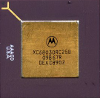
The PowerBook 100, 14x, and 170 use a different LCD driver chip called Omaha2 (U4 on the CPU board), which we know is called Omaha2 because it's labeled on the schematic. Omaha2 is located on the PCB board and is the same chip on passive matrix and active matrix systems. Omaha2 is almost the same as Omaha, but adds STN_MODE and a special STN_CLK as an input, and is capable of generating its own M signal. Omaha2 is called the DDC (Display Driver Chip) in the 140/170 dev note, but Apple stopped giving detailed explanations of how it works. I assume this is because they weren't breaking out the signals on an external connector anymore.
The PowerBook 16x and 180 use a completely different chip that Apple calls the GSC (Gray Scale Controller) in the 160/180 dev note. GSC adds support for grayscale, of course, and 128K of VRAM instead of 32K. There's no schematics available for these models that I can find, but I have done some original research.
Omaha, Omaha2, and GSC all have 16-bit data interfaces that are also byte addressable. Keeping GSC on a 16-bit interface seems kind of tight, considering that it has to handle up to 4x the amount of data as Omaha and Omaha2.
The same LCD driver chip is used on all versions of in-family CPU boards, but it is connected to active-matrix and passive-matrix displays. The STN_MODE pin is pulled up on the CPU board, and if you inspect the back of an active-matrix display, you can see that pin 23, STN_MODE, is connected to the ground plane. STN_MODE measures 5V (logic 1) when a passive-matrix display is connected, and thus tells the video chip whether a passive-matrix ((F)STN) or active-matrix display is connected. As a result, we can conclude that the two display types require different signals, and this is observable if you power a PowerBook with no display attached and change the logic level on STN_MODE. What can we conclude from this? Well, for one (ignoring the inverter boards), all monochrome/grayscale displays are compatible with all monochrome/grayscale PowerBooks, assuming you have the right display cable. The video chip is told how to drive the connected display, and there's no way to tell that chip if a passive-matrix Rev. A, B, C, or some other display is connected---all it knows is if the display is active or passive. Additionally, GSC and Omaha(2) have the same amount of information about the connected display, so any screen from a monochrome computer should be compatible with a grayscale computer, and vice versa. The one caveat with this is that it's possible that, for example, Apple chose passive-matrix Rev. A displays before they decided that future computers would have grayscale support, and thus Rev. A displays don't support grayscale, but I doubt this. If somebody would like to test, I'd be interested in the results! I only have one Rev. C display and it works in both my 145B and my 160.
I have so far figured out Omaha2's data format in passive matrix mode, so that will be my next post.
Let's start with the display. The schematics for the 14x/170 are available and include the pinout of the interconnect cable and connector, so I mapped out the pins on my 145B's interconnect board with my multimeter. The pinout is as follows (the underside of the interconnect board numbers the pins on every connector, helpfully):
| 1 | GND | 10 | GND | 19 | M_F |
| 2 | FPDATA[7] | 11 | FPDATA[1] | 20 | 5V |
| 3 | FPDATA[6] | 12 | FPDATA[0] | 21 | 5V |
| 4 | GND | 13 | GND | 22 | Inverter board pin 10 |
| 5 | FPDATA[5] | 14 | CL2I | 23 | STN_MODE |
| 6 | FPDATA[4] | 15 | GND | 24 | GND |
| 7 | GND | 16 | CL1I | 25 | DISP_BLANK/ |
| 8 | FPDATA[3] | 17 | GND | 26 | Inverter board pin 9 |
| 9 | FPDATA[2] | 18 | FLM_F |
The signal names are taken from the 140/170 schematics, and they're fairly sensible so I'll use them too. You can see the direct lineage from the Macintosh Portable here: the Portable exposes its LCD driver pins on its external video connector, but it branches them off from the driver chip and LCD through ferrites. The internal clock signals end with the letter I, like CL2I, and the external signals end with an X. Obviously the PowerBooks keep their LCD signals exclusively internal, but Apple kept the "I" in the names. I don't keep the I around except for direct reference to the schematic. A slash at the end of a name indicates an active-low signal.
These signals are:
- FPDATA: an 8-bit data bus
- CL2, CL1, FLM_F, M_F: clocks
- STN_MODE: binary signal telling the video chip what kind of display is connected, see below
- DISP_BLANK/: display blanking signal from the Power Manager
- Inverter board pins: as far as I can tell, the contrast potentiometer is directly connected to the display. I suspect the high-voltage drive circuit is controlled by it.
The PowerBook 100, 14x, and 170 use a different LCD driver chip called Omaha2 (U4 on the CPU board), which we know is called Omaha2 because it's labeled on the schematic. Omaha2 is located on the PCB board and is the same chip on passive matrix and active matrix systems. Omaha2 is almost the same as Omaha, but adds STN_MODE and a special STN_CLK as an input, and is capable of generating its own M signal. Omaha2 is called the DDC (Display Driver Chip) in the 140/170 dev note, but Apple stopped giving detailed explanations of how it works. I assume this is because they weren't breaking out the signals on an external connector anymore.
The PowerBook 16x and 180 use a completely different chip that Apple calls the GSC (Gray Scale Controller) in the 160/180 dev note. GSC adds support for grayscale, of course, and 128K of VRAM instead of 32K. There's no schematics available for these models that I can find, but I have done some original research.
Omaha, Omaha2, and GSC all have 16-bit data interfaces that are also byte addressable. Keeping GSC on a 16-bit interface seems kind of tight, considering that it has to handle up to 4x the amount of data as Omaha and Omaha2.
The same LCD driver chip is used on all versions of in-family CPU boards, but it is connected to active-matrix and passive-matrix displays. The STN_MODE pin is pulled up on the CPU board, and if you inspect the back of an active-matrix display, you can see that pin 23, STN_MODE, is connected to the ground plane. STN_MODE measures 5V (logic 1) when a passive-matrix display is connected, and thus tells the video chip whether a passive-matrix ((F)STN) or active-matrix display is connected. As a result, we can conclude that the two display types require different signals, and this is observable if you power a PowerBook with no display attached and change the logic level on STN_MODE. What can we conclude from this? Well, for one (ignoring the inverter boards), all monochrome/grayscale displays are compatible with all monochrome/grayscale PowerBooks, assuming you have the right display cable. The video chip is told how to drive the connected display, and there's no way to tell that chip if a passive-matrix Rev. A, B, C, or some other display is connected---all it knows is if the display is active or passive. Additionally, GSC and Omaha(2) have the same amount of information about the connected display, so any screen from a monochrome computer should be compatible with a grayscale computer, and vice versa. The one caveat with this is that it's possible that, for example, Apple chose passive-matrix Rev. A displays before they decided that future computers would have grayscale support, and thus Rev. A displays don't support grayscale, but I doubt this. If somebody would like to test, I'd be interested in the results! I only have one Rev. C display and it works in both my 145B and my 160.
I have so far figured out Omaha2's data format in passive matrix mode, so that will be my next post.


") .
.