-
 Hello Guest! We're hosting a challenge to welcome vintage Intel macs to the MLA during the month of July! See this thread for more information.
 -
We've made some quality of life improvements to the Trading Post. More info here.
You are using an out of date browser. It may not display this or other websites correctly.
You should upgrade or use an alternative browser.
You should upgrade or use an alternative browser.
LC475 with no video
- Thread starter falen6
- Start date

when i suspected cap goo breaking connections I started reflowing pins - this chip was the first
i may have reflowed it twice ( maybe i missed one mentality )
allot of cap goo plus 2 bouts of heat did not fare out well
saying that i have had to reflow pins/pads on other boards several times without pads lifting
i put it down to sustained heat on a small pad is bad ........... sustained heat on a pad that has been 'electrolighted' is very very bad........
to them blast the whole area with a heat gun ................ ah well
----------------
there is basically zero clearance under these ram chips to run jumper wires under them , unless i start bending the pins to create more clearence
dont really want to go there
thats why im thinking of of using sticky copper tape - top left 3 pads missing , im thinking - prep the vias ( tiny sharp pin , dig out the via , file sharp point on soledring iron , flux / solder iron get good via contact - lay copper tape over the 3 missing pads and cover top half of vias - with sharp scalpal knife cut away the copper inbetween to create 3 new pads and traces - finish by soldering copper trace to via )
has anyone had any success with this method
i know i could just start running jumper wires from all over the place , including the back of the board but it be fugly
at least there are several pads that still look good , that will hold the chip solid , so the new connections wont be load bearing
imagine ...... it still gives a good chime !! , and not with just the chip removed , but the 2 caps as well !!!
SMD packages don't sit completely flush to the board. If you use #32 bare wire there should be plenty of clearance.there is basically zero clearance under these ram chips to run jumper wires under them , unless i start bending the pins to create more clearence
dont really want to go there
i was looking at a small transformer off some board i have in a drawer - the wire thats wound onto that is very fine .... and the would be insulated as well - that would be a much easier way to go shircshSMD packages don't sit completely flush to the board. If you use #32 bare wire there should be plenty of clearance.
wont be going at it for a few days - have to change a blown head gasket on my car tomorrow - cant wait !!!
Regarding the onboard RAM, is this possible to disable it entirely, so that only the SIMM is used ?
Edit: this seems possible but requires a ROM modification
Edit: this seems possible but requires a ROM modification
For those with LC475/Q605-type Macs (ROM checksum FF 74 39 EE), a working SIMM slot, a SIMM programmer, and an available 8MB SIMM..... I would appreciate feedback on the attached ROM.
Firstly, thanks goes to @JDW @Jockelill and @WillJac for doing some initial testing and providing feedback. An important lesson we learned during testing is to fully reset your PRAM before using a new ROM. Especially if the new ROM uses PRAM settings (such as this one).
Secondly, I want to specifically point out that I am using a modified version of the CDEV (control panel) that...
- frontein1
- Replies: 38
- Forum: Mac II, Quadra & Centris
ive no idea - but its a great idea - ............in rom , yes i guess........... wouldnt it be great if the desigeners included a jumper to bypass the onboard ram
i wonder if there is a way to do it , to trick the rom .......... to not have to replace roms ........... some simple way to report 'onboard ram not present , but keep going ROM"
that might just reserect many lc475's
i wonder if there is a way to do it , to trick the rom .......... to not have to replace roms ........... some simple way to report 'onboard ram not present , but keep going ROM"
that might just reserect many lc475's

Just leave it off, don't need to do anything fancy. Desolder it.Regarding the onboard RAM, is this possible to disable it entirely, so that only the SIMM is used ?
The ROM hacks are for disabling it without removing it.
I have the onboard RAM removed from a couple of my machines. A 610 and a 650. Both which basically use a closely related Memory Controller.
I thought @dougg3 discovered that the right type of ROM SIMM automatically disables the onboard chips
Maybe you’re referring to this very instructive blog from @dougg3 ?
Downtown Doug Brown » Revisiting programmable Mac ROM SIMMs in Quadras
As I understand it, he discusses more a way to disable the onboard ROM
Very interesting thanks. That’s a simple solution indeed.Just leave it off, don't need to do anything fancy. Desolder it.
The ROM hacks are for disabling it without removing it.
Maybe there is a subtle way to desolder just a few pins without desoldering the chips completely.
That would require to study the schematics
https://macdat.net/files/pdf/apple/schematics/apple/lc475.pdf
I was. I got confused and thought someone was trying to disable the onboard ROM but see now they were talking about RAM.Maybe you’re referring to this very instructive blog from @dougg3 ?
Downtown Doug Brown » Revisiting programmable Mac ROM SIMMs in Quadras
www.downtowndougbrown.com
As I understand it, he discusses more a way to disable the onboard ROM
Got my car done , finally getting back to this poor LC
I need some help folks - cant read schematics .... not a clue
trying to understand them
looking at U5 on this schematic i dont understand what " DADDR[0] 9 A0 " means - what bloody pin is this on the chip
dont the pin counts start at 1 , going anti clockwise , so the "A0" part is not the pin number ( im guessing A0 to A9 is a data bus .... a 10 bit data bus ? ) ....... i hav no idea how to read these
I was thinking the '9' before it could be a pin number on the chip , but then as you go down the values on the left side I see the numbers 22 , 23 ........ how can they be pin numbers on a 20 pin chip
for the love of god , someone please tell me which number from " DADDR[0] 9 A0 " refers to the actual pin on the chip
i notice there are 20 lines coming from the chip in the schematic so if i take them as "DADDR[0] 9 A0" being pin 1 then pin 20 would be the 'line' coming from the top of the graphic ........ going on this i thought pins 13 and 15 were going to ground ( as i see the ground symbol) , but they dont appear to be ......... pin 20 ( the one from the top of the graphic) is the ground........... ?????
using simple continuity tests from U7 to its neighbouring ram chips i start to see the many pins are connected to the same pins on each ram chip - i guess this is the data bus the schematic shows ( A0 to A9) ...........until you get to U11....... i see many traces broken on U11 as well as U5
so the electrolite got up as far as the second ram chip from the caps and broke some traces on that chip as well
if i ever get this board working ........... it aint gonna be pretty with the amount of jumper wires i will have to run

does anyone have a picture of an LC475 board with the ram chips removed...i just need to see the traces
I need some help folks - cant read schematics .... not a clue
trying to understand them
looking at U5 on this schematic i dont understand what " DADDR[0] 9 A0 " means - what bloody pin is this on the chip
dont the pin counts start at 1 , going anti clockwise , so the "A0" part is not the pin number ( im guessing A0 to A9 is a data bus .... a 10 bit data bus ? ) ....... i hav no idea how to read these
I was thinking the '9' before it could be a pin number on the chip , but then as you go down the values on the left side I see the numbers 22 , 23 ........ how can they be pin numbers on a 20 pin chip
for the love of god , someone please tell me which number from " DADDR[0] 9 A0 " refers to the actual pin on the chip
i notice there are 20 lines coming from the chip in the schematic so if i take them as "DADDR[0] 9 A0" being pin 1 then pin 20 would be the 'line' coming from the top of the graphic ........ going on this i thought pins 13 and 15 were going to ground ( as i see the ground symbol) , but they dont appear to be ......... pin 20 ( the one from the top of the graphic) is the ground........... ?????
using simple continuity tests from U7 to its neighbouring ram chips i start to see the many pins are connected to the same pins on each ram chip - i guess this is the data bus the schematic shows ( A0 to A9) ...........until you get to U11....... i see many traces broken on U11 as well as U5
so the electrolite got up as far as the second ram chip from the caps and broke some traces on that chip as well
if i ever get this board working ........... it aint gonna be pretty with the amount of jumper wires i will have to run
does anyone have a picture of an LC475 board with the ram chips removed...i just need to see the traces
DADDR[0] is the signal name, 9 is the pin number (like normal, but not shown in position on the schematic to make it easier to avoid having to cross lines over) and A0 is the chip pin name.DADDR[0] 9 A0
Oh, yeah... Things are a bit weird sometimes.Thanks for that Phipli
But if 9 is the actual pin number ( from DADDR[0] 9 A0 ) then what pin is "IO4 25 D(31)" or "VSS 26" - theres only 20 pins on these ram chips , there is no pin 25 or 26
so sorry for my cluelessness on these schematics
See the gaps with no pins? Those are counted as 3 pins per side. So the pin count goes... 1,2,3,4,5,-,-,-,9,10,11,12,13,14,15,16,17,18,-,-,-,22,23,24,25,26...
Obviously isn't it?

oh man........ i give up on schematics ......... there are just simply things in life that some of us are not meant to understand - i have sat and watched tutorials on schematics , many times , and just gave up each time
im slowly trying to map out the traces

many breaks in traces from U5 to U11 , from U5 pins to the vias ....... the electrolite really chewed up the traces
i will have to test all of the vias in the area of U5 for continutity to the other side of the board - half the solder is missing from the vias as they are rotted out
im slowly trying to map out the traces
many breaks in traces from U5 to U11 , from U5 pins to the vias ....... the electrolite really chewed up the traces
i will have to test all of the vias in the area of U5 for continutity to the other side of the board - half the solder is missing from the vias as they are rotted out
Attachments
Last edited:
Don't give up, you'll get used to it with time. The apple ones are easier to read than some, so aren't too bad to learn with (the Bomarc ones are a nightmare).oh man........ i give up on schematics ......... there are just simply things in life that some of us are not meant to understand - i have sat and watched tutorials on schematics , many times , and just gave up each time
im slowly trying to map out the traces
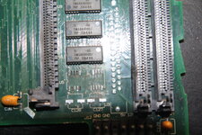
View attachment 98346
many breaks in traces from U5 to U11 , from U5 pins to the vias ....... the electrolite really chewed up the traces
i will have to test all of the vias in the area of U5 for continutity to the other side of the board - half the solder is missing from the vias as they are rotted out
well - tried to run jump wires , all over the place
turned out to be impossible
vias were too small - i did manage to solder wires into the vias but there were so many breaks in the traces i was just knocking off wires i already soldered while trying to add more jumpers
you would need a microscope for this much rewiring
i should have tried using sticky copper tape and carve out the new traces and pads - i have never tried it but after the amount of time i spent trying to solder jump wires i believe it would have sooo much easier to use sticky back copper tape
this one is going straight back up into the attic ............ and staying there
thanks for the help folks
So, I'd really be surprised if there were more than a couple of broken traces. I'd be very careful that you're not mistaking things that aren't connected. Attic might be a good idea, but remove the jumpers you've added first.well - tried to run jump wires , all over the place
turned out to be impossible
vias were too small - i did manage to solder wires into the vias but there were so many breaks in the traces i was just knocking off wires i already soldered while trying to add more jumpers
you would need a microscope for this much rewiring
i should have tried using sticky copper tape and carve out the new traces and pads - i have never tried it but after the amount of time i spent trying to solder jump wires i believe it would have sooo much easier to use sticky back copper tape
this one is going straight back up into the attic ............ and staying there
thanks for the help folks
well i had 3 missing pads top left with vias just below them - i managed to solder wire from via to the pin , on all 3
but there were 6 pins that were not connected to their vias below the chip ( in the picture ) - they also did not connect to their corresponding chip above - so 2 breaks for each - 12 breaks ...... then i found that there were 3 more breaks from U11 to the next ram chip above .......
the 6 breaks on U5 alone were breaks , as i had the chip removed and was looking at the pad , the trace , the via , the trace also running to U11 ....... all broken
at first i reflowed all 20 pins - then did it again - then removed the chip - using hot air to remove the chip made things worse as it came away from the board with 4 or 5 pads on the pins !!!
and i have removed many many chips in the past with no damage
what i was trying to do was solder tiny wire from via to pin , then solder a second wire from same pin to coresponding pin on the next chip above
this is not the way to go for this ......... your trying to solder on a second tiny wire to a pin with a wire you already have attached and end up knocking off the wire you already had in place , sometimes wires on the pins either side ........... a dam nightmare
Similar threads
- Replies
- 0
- Views
- 310