• Hello MLAers! We've re-enabled auto-approval for accounts. If you are still waiting on account approval, please check this thread for more information.

help on macintosh SE/30

Hello everyone,

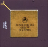
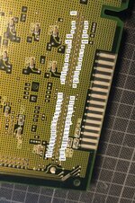
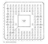
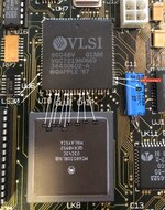
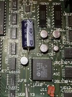
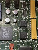
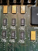
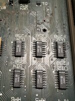
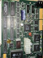
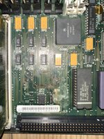
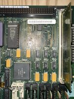
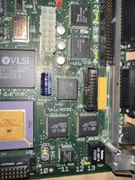
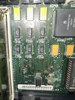
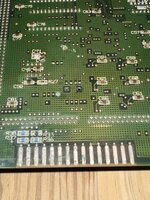
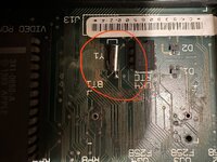
I found a Macintosh SE/30, removed the motherboard, cleaned it, and then tried to turn it on. Here is the result. Can any experts diagnose, or at least isolate, the problem from this symptom? I have read various things about simasimac, but it seems to be a different pattern.

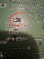
Could it just need a recap, or...?

No chime at start-up.


se30.jpg
 
I’m hardly an expert but You’ll definitely need to do a complete recap and check all the traces to make sure. You could also check the ROM SIMM is not loose and is seated correctly.
 
You will certainly need to do a recap! Do you have a picture of the logic board? I'd carefully inspect and clean everything around UD8, UE8 etc..
Where in Switzerland are you located?
 
Ok, I did some research and I found out that some connections between the ROM and the CPU are broken. According to the scheme I posted below I find out that 5 traces are broken (D0, D10, D9, A12, A18). But the ones on the glue chip are all good, at least the ones the guy who did this research pointed out in his work (his problem was just the red pin on the Glue chip. Actually, I'm referring to his job as I'm not an expert...
Could be this the problem? well, I suppose yes if not also others.
So, I'm planning to make some jump wires to reconnect those traces. Any advise on this work will be really welcome. As I said I'm not really an expert, but anyway, I rebuild a flat cable of my powerbook 180c, so I can manage a little bit - see the picture of this work below. I'm quite proud of it ;-)

I also post some pictures of the board, I took pics on the most damaged/corroded areas to give the idea. what i'm asking to experts is: is the board good enough to work or is just a waste of time recapping and rewire those pins?.
 

Attachments

  • rom-socket-matching.jpg
    rom-socket-matching.jpg
    1.5 MB · Views: 30
  • Screenshot 2025-11-28 alle 21.42.42.png
    Screenshot 2025-11-28 alle 21.42.42.png
    285.6 KB · Views: 30
  • a24-trace.jpg
    a24-trace.jpg
    1.2 MB · Views: 40
  • IMG_9282 - dimensioni grandi.jpeg
    IMG_9282 - dimensioni grandi.jpeg
    363.5 KB · Views: 44
Ok, I did some research and I found out that some connections between the ROM and the CPU are broken. According to the scheme I posted below I find out that 5 traces are broken (D0, D10, D9, A12, A18). But the ones on the glue chip are all good, at least the ones the guy who did this research pointed out in his work (his problem was just the red pin on the Glue chip. Actually, I'm referring to his job as I'm not an expert...
Could be this the problem? well, I suppose yes if not also others.
So, I'm planning to make some jump wires to reconnect those traces. Any advise on this work will be really welcome. As I said I'm not really an expert, but anyway, I rebuild a flat cable of my powerbook 180c, so I can manage a little bit - see the picture of this work below. I'm quite proud of it ;-)

I also post some pictures of the board, I took pics on the most damaged/corroded areas to give the idea. what i'm asking to experts is: is the board good enough to work or is just a waste of time recapping and rewire those pins?.

The flat flex cable is amazing, well done!

By all means a repair is worth doing on this SE/30 board, the only time it might not be is if it's had moderate to severe battery damage.
 
here is ma board
 

Attachments

  • IMG_9431 - dimensioni grandi.jpeg
    IMG_9431 - dimensioni grandi.jpeg
    387.1 KB · Views: 42
  • IMG_9432 - dimensioni grandi.jpeg
    IMG_9432 - dimensioni grandi.jpeg
    372 KB · Views: 30
  • IMG_9433 - dimensioni grandi.jpeg
    IMG_9433 - dimensioni grandi.jpeg
    374.7 KB · Views: 29
  • IMG_9434 - dimensioni grandi.jpeg
    IMG_9434 - dimensioni grandi.jpeg
    450.9 KB · Views: 32
  • IMG_9439 - dimensioni grandi.jpeg
    IMG_9439 - dimensioni grandi.jpeg
    401.5 KB · Views: 30
  • IMG_9438 - dimensioni grandi.jpeg
    IMG_9438 - dimensioni grandi.jpeg
    368.8 KB · Views: 27
  • IMG_9436 - dimensioni grandi.jpeg
    IMG_9436 - dimensioni grandi.jpeg
    356.6 KB · Views: 30
  • IMG_9440 - dimensioni grandi.jpeg
    IMG_9440 - dimensioni grandi.jpeg
    372 KB · Views: 26
  • IMG_9441 - dimensioni grandi.jpeg
    IMG_9441 - dimensioni grandi.jpeg
    350.8 KB · Views: 26
  • IMG_9447 - dimensioni grandi.jpeg
    IMG_9447 - dimensioni grandi.jpeg
    312.6 KB · Views: 36
Oh, it is battery damaged. OK, that explains the many broken traces. I would certainly have a go at repairing it, what's to lose?
 
Well I never recap anything, hope is not too difficult...

seem that someone already work on that board, the battery was not the original one and i see some corrosion on that area, not too bad in my opinion but I actually cannot judge. maybe some more expert than me can tell better than me
 

Attachments

  • IMG_9443.jpg
    IMG_9443.jpg
    1.1 MB · Views: 36
  • IMG_9444.jpg
    IMG_9444.jpg
    907.4 KB · Views: 37
Well I never recap anything, hope is not too difficult...

seem that someone already work on that board, the battery was not the original one and i see some corrosion on that area, not too bad in my opinion but I actually cannot judge. maybe some more expert than me can tell better than me

I think you will be able to handle the trace repair looking at your beautiful and intricate work on the PowerBook LCD cable.

I guess more important is whether you want to - as in, would you enjoy the challenge?

Recapping will be the easy part... and is good practice anyway. I recommend the 'twist' method to remove the old surface-mount ones: grab each one with a pair of needle nose pliers and twist (rotate) back and forwards until they fall off. Then you can clean up the pads.
 
Oh, it is battery damaged. OK, that explains the many broken traces. I would certainly have a go at repairing it, what's to lose?
yes, but seem worst on pictures. Most of what you see is a surface layer of what remains from the battery leak, which I can't remove even with IPA. When wet, you can clearly see the intact connections, but not all of them will be intact.
 
I think you will be able to handle the trace repair looking at your beautiful and intricate work on the PowerBook LCD cable.

I guess more important is whether you want to - as in, would you enjoy the challenge?

Recapping will be the easy part... and is good practice anyway. I recommend the 'twist' method to remove the old surface-mount ones: grab each one with a pair of needle nose pliers and twist (rotate) back and forwards until they fall off. Then you can clean up the pads.
Looking at the board, do you think that once that ROM-CPU connections will be done the Mac would work again? what about that green corrosion on some chips? terrible or what?
 
Looking at the board, do you think that once that ROM-CPU connections will be done the Mac would work again? what about that green corrosion on some chips? terrible or what?

Possibly - it depends if the corrosion has damaged any vias or internal traces.

The green corrosion I can see on the ASC and SCSI chips for example doesn't worry me very much, it's just on the surface, and could be cleaned off. The F258s and yellow Bourns filters with dull legs near the battery I would swap out with new ones, however.
 
Ok… rewiring cpu-rom pins is done. Shall I give a try, still with old caps, or better not to?
 

Attachments

  • IMG_9458.jpeg
    IMG_9458.jpeg
    1.9 MB · Views: 13
And what about those big pads? What are intended for? Shall I put some new solder on them?
 

Attachments

  • IMG_9459.jpeg
    IMG_9459.jpeg
    2.3 MB · Views: 11
  • IMG_9460.jpeg
    IMG_9460.jpeg
    2.7 MB · Views: 6
A question about recap: tantalum or cans? Wich are the easiest so solder? This is my only concern. I do not care if they will last just 40 years and not 140…

Thanks for your help on this
 
Big pads were probably used at the factory for testing purposes, you can skip any work to them.

I will try with basic capacitors for tests, then once up and running will go with good ones.
 
Big pads were probably used at the factory for testing purposes, you can skip any work to them.

Yes, correct.

I will try with basic capacitors for tests, then once up and running will go with good ones.

Agreed - running it for a short time won’t be an issue.

A question about recap: tantalum or cans? Wich are the easiest so solder? This is my only concern. I do not care if they will last just 40 years and not 140…

Tantalums are probably easier to solder since they have wide conductive terminals as opposed to the legs of tin cans which don’t protrude very much from the plastic base. However, some tantalums are a bit too long for the footprints on the board - they might overlap the pads too much - so make sure you measure first.

Also, make sure you select 25v caps for all the 47uF parts as tantalum needs to be derated (basically it needs more headroom than electrolytic).

Take special care with C10 as it sees 12V and runs next to some data lines. I would position (offset) the cap nearer to the J12 power connector so that the relatively wide terminals of the tantalum cap are not sticking out further than the pads themselves on the side of those data lines. If those get bridged with the cap it will destroy half the chips on the board. This can happen if the solder mask is missing above the traces and the cap bridges it. It’s mostly an issue for people using ceramic caps (which I would
never recommend), but worth bearing in mind for tantalums too.
 
Last edited:
Yes, correct.


Agreed - running it for a short time won’t be an issue.


Tantalums are probably easier to solder since they have wide conductive terminals as opposed to the legs of tin cans which don’t protrude very much from the plastic base. However, some tantalums are a bit too long for the footprints on the board - they might overlap the pads too much - so make sure you measure first.

Also, make sure you select 25v caps for all the 47uF parts as tantalum needs to be derated (basically it needs more headroom than electrolytic).

Take special care with C10 as it sees 12V and runs next to some data lines. I would position (offset) the cap nearer to the J12 power connector so that the relatively wide terminals of the tantalum cap are not sticking out further than the pads themselves on the side of those data lines. If those get bridged with the cap it will destroy half the chips on the board. This can happen if the solder mask is missing above the traces and the cap bridges it. It’s mostly an issue for people using ceramic caps (which I would
never recommend), but worth bearing in mind for tantalums too.
Ok thanks.
 
Back
Top