• Hello MLAers! We've re-enabled auto-approval for accounts. If you are still waiting on account approval, please check this thread for more information.

Address mirroring on 128K/512K/Plus

Anyone know of a good source that describes how RAM and ROM are mirrored at different addresses on the Mac 128K, 512K, and Plus? I remember reading something about it a few weeks ago, possibly here, but can't find it now.

I'm not talking about the basic memory map, which is well documented, but the details of where mirrors of RAM/ROM appear elsewhere in the memory map besides their regular locations. For example, the 128K ROM on the Plus is at $400000-$41FFFF, but is probably also mirrored at $420000-$43FFFF, among other places.

I think I also read something here on this site that mentioned that the presence/absence of particular mirroring windows was used by the boot ROM to detect how much memory is installed, or whether a machine is a 512Ke or a Plus, or something like that.

 
Another closely related question is the use of the memory overlay feature during boot-up. According to a few sources I've read, at boot-up an overlay bit is set, which maps a copy of ROM to $000000, and moves RAM to $600000. Later during boot-up, after all the memory tests have been performed, the overlay bit is cleared and the normal address mapping is restored. Here's how it's described in http://www.mac.linux-m68k.org/devel/plushw.php:

First, the processor is held in a wait state while a series of circuits getsthe system ready for operation. The VIA and IWM are initialized, and the

mapping of ROM and RAM are altered temporarily by setting the overlay bit in

VIA data register A. This places the ROM starting at the normal ROM

location $400000, and a duplicate image of the same ROM starting at address

0 (where RAM normally is), while RAM is placed starting at $600000. Under

this mapping, the Macintosh software executes out of the normal ROM

locations above $400000, but the MC68000 can obtain some critical low-memory

vectors from the ROM image it finds at address 0.

Next, a memory test and several other system tests take place. After the

system is fully tested and initialized, the software clears the VIA's

overlay bit, mapping the system RAM back where it belongs, starting at

address 0. Then the disk startup process begins.
However, based on my examination and disassembly of the 128K Mac ROM, this is incorrect. Very early in the boot-up process, the overlay bit is cleared, well before any memory tests are performed. Furthermore, no RAM accesses are ever made while the overlay bit is set, so this whole RAM relocation to $600000 thing might as well never have happened.

Anyone familiar with this process? Could this be something that differs between the 64K and 128K ROM behaviors? I haven't tried disassembling the 64K ROM yet.

 
easiest thing i think would be just compile MESS to run on top of a kernel developed for your custom hardware? I know there are CPUs out there such as the ARM or MIPS type that have loads and loads of linux/unix kernels made for them, compile MESS on top of that, with the drivers written and linked into the kernel for your external devices, and video device. theres your mac. Thats how modern LCD/Plasma TVs are done. They use a CPLD/FPGA with an on-chip CPU (thinking of MiTek). all in one for the panel timings and etc.. running an embedded linux environment. Philips did exactly this. RGB LED signs are done in this fashon as well. FPGAs handle the LED timing, sustain, and color depth while the CPU runs all the scalar code and etc.

 
Well, the easiest thing would be to just run MESS on a PC. :)

It's all pointless nostalgia tech in the end, so there's not really a right or wrong way to do it, but I personally don't want to use an emulator. Running compiled C code on a general purpose CPU seems little different to me whether it's a PC's Core i7 or an ARM chip on a custom board. I really want to implement things at the hardware level, using a real CPU, with the FPGA replacing peripheral chips like the VIA and SCC. I've made some decent progress down that path so far, though there's still a long way to go!

 
Guide to the Macintosh Family Hardware 2nd Edition has this mirroring info. It also has info about /DTACK vs /VPA and some interesting info about how the OS reads an address in the "Phase read" range to make sure RAM addresses are timed right. If you want, I can scan some pages for you -- let me know (not sure if I'm allowed to post them directly on these boards). Here are a few useful excerpts:

Talking about the classic Macintosh computers (Plus and earlier):

The ROM overlay address map, used when the machine is turned on or reset, maps addresses from $00 0000 to $01 FFFF to locations in ROM rather than to RAM. The startup or Reset handler software switches from the ROM overlay address map to the normal address map by setting low the Overlay signal from the VIA.
They provide two memory maps for the 512k and two memory maps for the Plus (I'm assuming the 128k is counted as part of the 512k because they talk about 128k of RAM vs 512k of RAM and 64k of ROM vs 128k of ROM). I'm too lazy to turn $01 0000 into $00 FFFF and so on for the ending addresses of ranges, so make the ending addresses non-inclusive (except for the last one) :-)

I'm only typing up the 512k one for now but if you'd like the Plus one, I will definitely scan it for you. It's basically the same thing as the 512k map with a chunk eaten out of some of the address space for the SCSI, and some reserved sections next to the IWM and SCC stuff have been taken to be used by those peripherals, but there's some stuff going on in the RAM section that's kind of hard to type up.

512k Map on Power-up (OVERLAY=1)

$00 0000 to $01 0000 = Image of ROM (Original 64KB)

$01 0000 to $02 0000 = Image of ROM (Enhanced 128KB)

$02 0000 to $10 0000 = Repeated ROM images

$10 0000 to $20 0000 = No device assigned

$20 0000 to $30 0000 = More ROM images

$30 0000 to $40 0000 = No device assigned

$40 0000 to $41 0000 = ROM (Original 64KB)

$41 0000 to $42 0000 = ROM (Enhanced 128KB)

$42 0000 to $50 0000 = Repeated ROM images

$50 0000 to $52 0000 = Reserved

$52 0000 to $60 0000 = No device assigned

$60 0000 to $62 0000 = RAM (128 KB)

$62 0000 to $68 0000 = RAM (512 KB)

$68 0000 to $80 0000 = Repeated RAM images

$80 0000 to $90 0000 = Reserved

$90 0000 to $A0 0000 = Phase adjust (word) -- SCC reset (A0 = 1) or SCC read (A0 = 0)

$A0 0000 to $B0 0000 = Reserved

$B0 0000 to $C0 0000 = Phase adjust (word) -- SCC write (A0 = 1)

$C0 0000 to $D0 0000 = Reserved

$D0 0000 to $E0 0000 = IWM (A0 = 1)

$E0 0000 to $E8 0000 = Reserved

$E8 0000 to $F0 0000 = VIA (A0 = 0)

$F0 0000 to $F8 0000 = Phase read

$F8 0000 to $FA 0000 = Apple test software

$FA 0000 to $FF FFF0 = No device assigned

$FF FFF0 to $FF FFFF = Autovector read

512k Map Normal (OVERLAY=0)

$00 0000 to $02 0000 = RAM (128k)

$02 0000 to $08 0000 = RAM (128k)

$08 0000 to $40 0000 = Repeated RAM images

$40 0000 to $41 0000 = ROM (Original 64KB)

$41 0000 to $42 0000 = ROM (Enhanced 128KB)

$42 0000 to $50 0000 = Repeated ROM images

$50 0000 to $52 0000 = Reserved

$52 0000 to $80 0000 = No device assigned

$80 0000 to $90 0000 = Reserved

$90 0000 to $A0 0000 = Phase adjust (word) -- SCC reset (A0 = 1) or SCC read (A0 = 0)

$A0 0000 to $B0 0000 = Reserved

$B0 0000 to $C0 0000 = Phase adjust (word) -- SCC write (A0 = 1)

$C0 0000 to $D0 0000 = Reserved

$D0 0000 to $E0 0000 = IWM (A0 = 1)

$E0 0000 to $E8 0000 = Reserved

$E8 0000 to $F0 0000 = VIA (A0 = 0)

$F0 0000 to $F8 0000 = Phase read

$F8 0000 to $FA 0000 = Apple test software

$FA 0000 to $FF FFF0 = No device assigned

$FF FFF0 to $FF FFFF = Autovector read
 
Well, the easiest thing would be to just run MESS on a PC. :)
It's all pointless nostalgia tech in the end, so there's not really a right or wrong way to do it, but I personally don't want to use an emulator. Running compiled C code on a general purpose CPU seems little different to me whether it's a PC's Core i7 or an ARM chip on a custom board. I really want to implement things at the hardware level, using a real CPU, with the FPGA replacing peripheral chips like the VIA and SCC. I've made some decent progress down that path so far, though there's still a long way to go!
Hey, There is nothing wrong with how you want to do it. nothing wrong with that at all. Its all in the matter of how you do it and how well you enjoy it. :-) hopefully its all fun in the end. hehe.

i just threw an idea out there is all :-)

 
Awesome, thanks! Looks like I really should get a copy of that book. I'd already figured out much of what you described there, but some of it is new. If you wouldn't mind scanning the Plus memory map page too, that would be great.

512k Map Normal (OVERLAY=0)
$00 0000 to $02 0000 = RAM (128k)

$02 0000 to $08 0000 = RAM (128k)

$08 0000 to $40 0000 = Repeated RAM images
I'm guessing that was supposed to be be:

$02 0000 to $08 0000 = RAM (512k)
 
You're welcome! Yeah, you're right. That was a goofup on my part. I also meant to say "RAM accesses" not "RAM addresses".

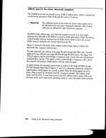
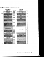
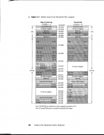
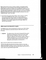
Here are the relevant pages (I made the chart pages bigger because they are kind of hard to read with the dark background):

122.png

123.png

124.png

125.png

 
Awesome! OK, I really need to get that book.

You can see the answer to my original question in the footnote on the Plus memory map diagram:

Note: 128 KB ROMs are disabled (no device assigned) everywhere A17=1.
So for a 512Ke, $020000-$03FFFF maps to a copy of the ROM, but on the Plus, that same address range is not mapped to anything.

 
Back
Top