• Hello Guest! We're hosting a challenge to welcome vintage Intel macs to the MLA during the month of July! See this thread for more information.
  • We've made some quality of life improvements to the Trading Post. More info here.

adding 4mb SGRAM to PowerPC 5500/6500 ... and possible ATi Rage Pro upgrade

So, Jeff graciously sent me a few KM4132G512Q-10 chips, they're 256 X 32 X 2 (2MB) each, while the chips already soldered on the 6500 are MT41LC256K32D4, 128 X 32 X 2 (1MB). I am adding both Data Sheets below.
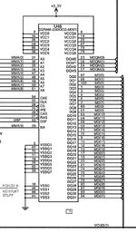
While the pin for BA, according to the 6500 schematic, is connected (they are both dual bank chips) the caveat here is that address lines A8 and A9 are, for some unfathomable reason, mapped on different pins on the MT and KM memory chips footprint which are otherwise essentially the same.
I will undoubtedly have to bodge some wires to solve this.

I was just looking at the datasheet for the km4132g512q and it needs 10 address lines (notice that pin 29 is now a10 rather than a9) whereas the Rage Pro only has 9 address lines according to the Gossamer and Columbus schematics.
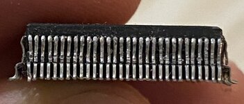
Piggy-backing chips (not easy with QFP - I tried) is the only way to do this.

IMG_9056.jpeg
 
Last edited:
It's a real pain that apple didn't do the standard arrangement of two chips with a socket for a module on top. That would have given us the same flexibility as the G3 with up to 6MB.
 
don't mind if I decided to finally look at the four datasheets I had for myself again while still not wanting to sleep yet (very lazy day so staying up awhile now heh) and hmm well I just have this to say for now..

Samsung KM4132G512 as per what the 6500 used has these particular pins;
29 - ba(a10)
30 - a8
51 - a9/ap [now this is a bit confusing as the datasheet doesn't explain what 'ap' is..]
58 - mch/nc [datasheet says 'mch' is for 'must connect high', I need to check the 6500 schematic tomorrow]

Micron MT41LC256K32D4 as tested in this forum thread;
29 - ba
30 - nc
51 - a8
58 - nc

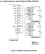
and I had been curious about the gpu datasheet having one figure diagram showing 512x32x2 which I had to try find something about on the web, eventually I tracked down an EtronTech EM636327 which has this pins;
29 - bs [datasheet says this is bank addressing so its the same bs=ba terminology after all]
30 - a8
51 - a9
58 - nc

so..going by that crude comparison list above its obvious that the etrontech doesn't need a pin30-to-pin51 bogey wire and that it has an a9 pin if the rage pro chip is actually utilizing that

I mean 4mbyte vram for 1024x768-in-millions-of-colour is more than reasonable, but nevertheless does anyone want to instead dream of 8mbyte for yer big back-breaking 1600x1200-in-millions-of-colour monitor nevertheless? hehe
 
don't mind if I decided to finally look at the four datasheets I had for myself again while still not wanting to sleep yet (very lazy day so staying up awhile now heh) and hmm well I just have this to say for now..

Samsung KM4132G512 as per what the 6500 used has these particular pins;
29 - ba(a10)
30 - a8
51 - a9/ap [now this is a bit confusing as the datasheet doesn't explain what 'ap' is..]
58 - mch/nc [datasheet says 'mch' is for 'must connect high', I need to check the 6500 schematic tomorrow]

Micron MT41LC256K32D4 as tested in this forum thread;
29 - ba
30 - nc
51 - a8
58 - nc

and I had been curious about the gpu datasheet having one figure diagram showing 512x32x2 which I had to try find something about on the web, eventually I tracked down an EtronTech EM636327 which has this pins;
29 - bs [datasheet says this is bank addressing so its the same bs=ba terminology after all]
30 - a8
51 - a9
58 - nc

so..going by that crude comparison list above its obvious that the etrontech doesn't need a pin30-to-pin51 bogey wire and that it has an a9 pin if the rage pro chip is actually utilizing that

I mean 4mbyte vram for 1024x768-in-millions-of-colour is more than reasonable, but nevertheless does anyone want to instead dream of 8mbyte for yer big back-breaking 1600x1200-in-millions-of-colour monitor nevertheless? hehe
It is pin 30 that isn't connected to anything on the board itself. So I guess you need a bodge wire for pin 30?

Edit - as @croissantking said, there are only MMA(0) to MMA(9) so you need to work out how to get an extra address line. I need to read more - how have people done it for stacked chips?

1000037283.jpg
 
Last edited:
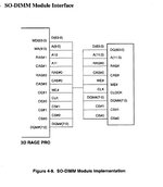
Ok, this bit of the Rage Pro datasheet looks pertinent:

1000037286.jpg

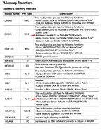
They use RAS#1 and CAS#1 as A10 and A11. (Look carefully because we have CS#0 and CAS#0 to confuse things).

These are NC on the 6500

1000037288.jpg

This is all confusing - I'd have thought CS 0 and 1 would be the missing lines where CS is chip select. I could do with reading more, but haven't long woken up.
 
Last edited:
That’s a game changer then - we could connect up RAS*1 to the new A10 pin.
Well done for finding that.
I just updated my post again, be aware I see but don't understand - I'm really groggy as I've only just woken up 😆

I'm confused why they break out the two CS lines but have labelled CAS and RAS #1 as the next address lines.
 
This is even more interesting for what we're talking about :

1000037290.jpg

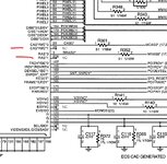
And helps because I can't find CS#0 and #1 on the 6500 schematic 😆
 
CS0 and CS1 are pins 112 and 110 respectively - you can see them near the GND and VCC pins. CS1 is tied high, CS0 is tied low.

But we can probably just ignore those.
 
This is exciting @Phipli as it looks like with 12 address lines we can have 8MB SGRAM right on the board with just a couple of bodge wires per chip.
If we can find some 512*32*2 chips :) know of any?

DQM for reference - not found the description yet :

1000037295.jpg

I really should make this datasheet searchable.
 
Back
Top