• Updated 2023-07-12: Hello, Guest! Welcome back, and be sure to check out this follow-up post about our outage a week or so ago.

ROM hack for 475/605 desired

Mustermann

Well-known member
I should have been more clear, the memory system will run at 40MHz too that way but it will use the timings that are intended for 33MHz operation.
They add more waitstates compared to the 25MHz settings.
U16 is used to read the state of the configuration resistors onto the data bus. The ROM holds tables for several memory speed configurations and the initialization code sets the appropriate values for each speed configuration.
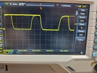
What happens is that you set the 40MHz configuration through the resistors which will tell the clock generator chip to output a 20MHz clock to the CPU clock generator resulting in 40MHz bus and CPU speed.
The problem is that there is no entry in the ROM table for the 40MHz setting hence it fails to post with that setting.

By lifting pin 11 on U16 and connecting it to ground the machine ID will be set to 33MHz and the appropriate memory timings will be used. The memory (both VRAM and RAM) will still be overclocked slightly that way.

If someone of the ROM wizards could modify that table to recognize the 40MHz setting and add the values that we know from the memory controller datasheet no further hardware modification would be necessary.
So it would be great to know, how to hack the ROM for this.
From my point of view there are two options:

Option1: Find all appropriate tables in ROM and add data for gestalt ID 91/96 (Maybe just copy gestalt ID 90/95)
So with changing the resistors and tables in the ROM, system is expected to work based on Bolle's post above.

Option2: Find the source code for reading the clock settings and change code so data for 40Mhz is the same than 33Mhz.
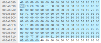
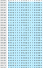
Someone may know the address where U16 (74F244) can be read.
Based on that the code in the ROM can be found where this address is read and add code.
So Mac ignore that clock pins has changed and operate in 33Mhz mode.

It seems that U16 provide data at D0-D3.

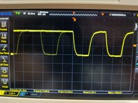
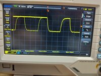
If address is not known, someone owning a logic analyzer may be able to read the address on bus when Gate of U16 is triggered.
 

eharmon

Well-known member
I believe @Jockelill thread covers the required updates to the tables via various links: https://68kmla.org/bb/index.php?threads/rom-hacking-in-the-68040-macs.46154/

Roughly, his link might just work out of box due to existing modifications. If not, you'll need to modify the tables as described by various postings (you can start from Jockelill's post) to teach the ROM how to apply 40MHz timings for different gestalt IDs.

FWIW it's "okay" to use the slower timings since they're looser...you'll just be leaving performance on the table.
 

Mustermann

Well-known member
Thank you for the link. I read thru it and the linked documents.

This is telling, how to implement
- a customizable ROM in 475/605 and many more (I have already ordered an universal ROM and a programmer)
- switch of RAM check and ROM checksum
- implementing ROM disk
- large RAM for Q650

Great work!

Unfortunately no hint, how to tweak gestalt ID or where programming tables for RAM are and how to change those.

That is why I am asking for.

@Bolle mentioned somewhere that there is documentation about the MEMC chip but I right now I only found some information about DJMEMC in emulator developement page: https://patchwork.ozlabs.org/project/qemu-devel/patch/20191212200142.15688-3-laurent@vivier.eu/

The most helpful I found was this thread https://68kmla.org/bb/index.php?threads/wombat-650-800-board-overclocking-limitations.38538/
But it is mostly about the DJMEMC used in 610/650/800. 475/605 uses a chip named as MEMCJR that might be different.

At page 11 you mentioned that you were hacking the LC 475 ROM directly to futz with even more customizing timings.
So you may know some details I was not able to understand from that thread yet.

It seems that some data for 40Mhz gestalt is missing in the 475/605 ROM.

My primary target right now is to enable 40Mhz without bending a leg of U16. Fine tune RAM timing might be nice to have.
 
Last edited:

Mustermann

Well-known member
Even if these are the tables, it doesn't make sense to me:
 

Attachments

  • DJMEMCTABLE.png
    DJMEMCTABLE.png
    57.7 KB · Views: 5
  • CPUIDPRODUCTLOOKUP.png
    CPUIDPRODUCTLOOKUP.png
    238.5 KB · Views: 7

eharmon

Well-known member
I found this helpful as well, but about DJMEMC as well: https://github.com/cy384/wombat-hacks/tree/main
You’re looking for https://github.com/cy384/wombat-hacks/tree/main/rom-hacking, specifically. Those have partially annotated tables, and the other values surround those regions so they can be modified as well. By adjusting and running the re-assembler you can get a rom with the new tables.

I’m not well versed in the 475 but I suspect memcjr configuration tables should be in that region as well.

I can take a poke to see if anything is obvious to me, though I have no way of testing so I can only give a cursory glance.
 

Mustermann

Well-known member
https://github.com/cy384/wombat-hacks/tree/main/rom-hacking
helps a lot for disassembly and assembly of a ROM.
Unfortunately the annotated-rom.S is out of a Wombat ROM that is different from a LC475 ROM and the annotated parts are about Wombat mostly.

I found this article that gave me the first hook:

Based on that LC475 and Q605 can be determined from machine ID register at 0x5ffffffc.

So I started to search my LC475 ROM for 0x5ffffffc.
When started ROM is located at 0x40800000 in LC475.

I found 0x5ffffffc at:

0x40804874
0x4080489C
0x40804948
0x40804BE6
0x40881C0C
0x408A014C
0x408A0574

Based on Quadra605ROM.lst.txt those are located in

MEMORYCTRLINITPATCH
0x40804874
0x4080489C
0x40804948

GETHARDWAREINFOPATCH
0x40804BE6

INITMMU
0x40881C0C

SIZEMEMORYPATCH
0x408A014C
0x408A0574

I disassembled MEMORYCTRLINITPATCH and found code to initialize Wombat boards and "other"
Tables djConfigTable, djRefreshTable, BIOS_Config, and BIOS_Timeout mentioned in https://github.com/cy384/wombat-hacks/tree/main/rom-hacking were found in MEMORYCTRLINITPATCH with same or similar values and another one that is similar to djConfigTable but with different values in some enties.

(Do not forget: All I found is from LC475 ROM)
 

Mustermann

Well-known member
I was not able to read content of 0x5ffffffc with the debugger so I need to assume two things:

Assumption 1: I can not read 0x5ffffffc because of MMU configuration.
Assumption 2: The bit of Q605 Jumper and the two bits for clock speed are mapped into the lowest 4 bit of 0x5ffffffc.

Assumption 2 is supported by the fact that LC457 has 0xa55a0x2221 in machine ID register and Q605 has 0xa55a2226
which differs in bit 3 (if counted from 1) which is exactly where the Jumper is connected to U16 (74F244).
Clock speed selectors are at bit 1 and 2 (if counted from 1).
 

Mustermann

Well-known member
Next question to answer is: What is ROM doing in MEMORYINITPATCH based on the MachineID read from $5FFFFFFC?

First read at $5FFFFFFC does not take care about the least significant bits, but do something for some specific machines.
40804872: MEMORYCTRLINITPATCH+$000C: LEA $5FFFFFFC,A2
40804878: MEMORYCTRLINITPATCH+$0012: MOVE.L (A2),D3
4080487A: MEMORYCTRLINITPATCH+$0014: ANDI.L #$0000FF00,D3 ; mask everything except of 2 Byte for grouping Machines
....

Second one includes the least significant bits, but also only does some branches for specific machines.
4080489A: MEMORYCTRLINITPATCH+$0034: LEA $5FFFFFFC,A2
408048A0: MEMORYCTRLINITPATCH+$003A: MOVE.L (A2),D3
408048A2: MEMORYCTRLINITPATCH+$003C: ANDI.W #$07FF,D3
408048A6: MEMORYCTRLINITPATCH+$0040: CMPI.W #$0003,D3
408048AA: MEMORYCTRLINITPATCH+$0044: BEQ.S ^$408048BC ;MEMORYCTRLINITPATCH¹+$56
408048AC: MEMORYCTRLINITPATCH+$0046: CMPI.W #$0101,D3
408048B0: MEMORYCTRLINITPATCH+$004A: BEQ.S ^$408048BC ;MEMORYCTRLINITPATCH¹+$56
....

Third is the interesting one: First there is a branch for Wombat machines, doing something else. Then there is data read from tables based on the least significant bits of the MachineIDRegister, so if Assumption 2 is right, different data is read for each CPU clock speed.
40804946: MEMORYCTRLINITPATCH¹+$00E0: MOVE.L $5FFFFFFC,D0
4080494C: MEMORYCTRLINITPATCH¹+$00E6: CMPI.W #$2BAD,D0 ; Wombat devices contain $2BAD here
40804950: MEMORYCTRLINITPATCH¹+$00EA: BEQ.S ^$408049C4 ;MEMORYCTRLINITPATCH¹+$15E ; for Wombat devices jump
40804952: MEMORYCTRLINITPATCH¹+$00EC: LEA $50F0E000,A2
40804958: MEMORYCTRLINITPATCH¹+$00F2: MOVE.W D0,D3
4080495A: MEMORYCTRLINITPATCH¹+$00F4: SWAP D3
4080495C: MEMORYCTRLINITPATCH¹+$00F6: MOVE.W D0,D3
4080495E: MEMORYCTRLINITPATCH¹+$00F8: ANDI.W #$0003,D3 ; Mask everything except of CPU Clock Bits
....

At his line a 40Mhz LC475 can be forced to use the 33Mhz settings instead of 40Mhz by changing
ANDI.W #$0003,D3
into
ANDI.W #$0002,D3

Using this patch CPU does not take care about the least significant bit of MachineID address (which is assumed to contain least significant bit of clock selector) and will use either 20Mhz settings or 33Mhz settings depending on the second clock selector bit.
 

Mustermann

Well-known member
The LC475 ROM contains the tables listed below already known from the Wombat ROM. No bump configs found.


40804A20: MEMORYCTRLINITPATCH¹+$01BA:
$0101 ; 4*2 Byte Data MEMCConfig used for Wombats
$001A
$00A3
$02F4

40804A28: MEMORYCTRLINITPATCH¹+$01C2:
$011D ; 4*2 Byte Data MEMCRefresh
$016B ;
$01E7 ;
$0255 ;

40804A30: MEMORYCTRLINITPATCH¹+$01CA:
$01 ; 4*1 Byte Data MEMCIntleaveEnable or BIOS
$01
$00
$00

40804A34: MEMORYCTRLINITPATCH¹+$01CE:
$0280 ; 4*2 Byte Data BIOS Timeout
$01E0
$00D5
$0000
 
Last edited:

Mustermann

Well-known member
However, the LC475 uses its own config table with different values for 33Mhz and 40Mhz:

08049BC: MEMORYCTRLINITPATCH¹+$0156:
$0101 ; 4*2 Byte Data MEMCConfig used for LC475/Q605 (and maybe other)
$001A
$00DC
$02DC

Some of the registers in which the table values are written are in a different place in the LC475.

These tables can be changed for 40Mhz config as well.
 
Last edited:

Mustermann

Well-known member
I played arround with MEMCConfig.
Lowest 3 Bits are known as ROMspeed (As of Wombat description)

LC475@25Mhz starts with MEMCConfig = $001A which is 0000000000011010 wich is ROMSpeed 2

I put my scope to OE of ROM and determined length of low puls: 120ns which is command (40ns) + 2 waitstates (2*40ns) in a 25Mhz system.

Next I changed MEMCConfig gegisters to all values of ROM Speed:

ROMSpeed 0: System Crash
ROMSpeed 1: 80ns
ROMSpeed 2: 120ns
ROMSpeed 3: 160ns
ROMSpeed 4: 200ns
ROMSpeed 5: 240ns
ROMSpeed 6: 280ns
ROMSpeed 7: 320ns

So I verified access time to ROM is (1+ROMSpeed)*Lenght of clock cycle.

Based on that minimum ROMSpeed is easy to calculate from CPU clock and Access Time of ROM (if known)
 

Attachments

  • ROMSpeed1.jpg
    ROMSpeed1.jpg
    1.6 MB · Views: 4
  • ROMSpeed2.jpg
    ROMSpeed2.jpg
    1.5 MB · Views: 4
  • ROMSpeed3.jpg
    ROMSpeed3.jpg
    1.5 MB · Views: 2

Mustermann

Well-known member
There are two other timings to change:
RAM
VRAM

Which of the other parameters
dwcpw​
fastwr​
mhz33​
drcpw​
cyc2ta​
drpchg​
drpw​
affects what?
 

Mustermann

Well-known member
I learned from the linked post about the meaning of the parameters above:
https://68kmla.org/bb/index.php?threads/wombat-650-800-board-overclocking-limitations.38538/page-11 #211

DCAS Pulse Width-Writes: If a 1, adds a clock cycle to the width of the second thru forth DCAS pulse of a write burst access
Fast Write Enable: If a 1, enables 3 cycle initial DRAM write access
CPU Clock Speed: 1 for 33Mhz or higher, adds a wait state to RAM access
DCAS Pulse Width-Reads: If a 1, adds a clock cycle to the width of the second thru forth DCAS pulse of a read burst access
Two Cycle Interleave: Since MEMCjr does not support interleaved memory, read only.
DRAS Precharge Width: If 1 adds a clock cycle to the width of DRAS precharge time.
DRAS Pulse Width: If 1 adds a clock cycle to width od DRAS

I also learned from the MEMCjr datasheet, that the table used by LC475 contain exactly what is expected for 40Mhz oepration.

So there is a configuration for 40Mhz in LC475 ROM and it seems to be correct for RAM.

I found a hint in the datasheet as well that there is a configuration register for VRAM as well (Frame Buffer Configuration $F9800010) but I was not able to determine where ROM is setting this parameter.
Parameter contain:

VCAS Pulse Width
VRAS Pulse Width
VRAS Precharge
Write Access

Some of them should be different for 25Mhz and for 40Mhz.
Maybe that is the reason why 40MHz by changing resistors does not work.

But there are also some other limitations:
40Mhz need:
- 120ns ROM
- 80ns RAM
- 70ns VRAM
- MC88920 seems not to work at that speed and need to be replaced by MC88916DW80
- SCSI clock need to be connected to another pin (move a resistor)
 
Last edited:
Top