• Updated 2023-07-12: Hello, Guest! Welcome back, and be sure to check out this follow-up post about our outage a week or so ago.

Reverse Engineering the Color Classic AB

ironborn65

Well-known member
I want to try to reverse engineer the AB of the Color Classic, AFAIK there is not a schematics out there and it would be helpful for the community.
I never attempted this kind of project before, but I will learn a lot and I like the idea.

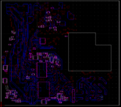
I have made an initial attempt starting from hi res pictures and creating a vector graphics using Corel Draw. I have 4 layers, 2 for the pictures and 1 for each of the 2 sides of the PCB. BTW I'm a MacOS kind of guy, of course!.
By now I have designed only the AC of the high power section. The result is terrible but I'm not sure I will go much further, it does not seem right to me. Corel Draw has not ready to be used electronics symbols and I have to create my own, dragging symbols around does not work and still I'm not sure if it will be possible to create a new PCB from it.
I read that another path is to transform the bitmap into vector graphics, I have made a quick attempt using Super Vectorizer Pro but the image tuning takes a lot of time and still the result is awful.
I could manually add the symbols using KiCad instead on top of the two pictures. The bottom side is plenty of SMD capacitors and resistors but it's doable IMO, it's not very complex.
I'm seeking here for suggestions from who already reversed a PCB in order to avoid trials and errors.
Which tool and process is recommend?
 

max1zzz

Well-known member
When creating straight copies of PCB's I generally favour Sprint layout, it allows you to import scans and trace over them and once you get used to it it is quick and easy to use however it has a couple of drawbacks - it dosen't create any kind of netlist or have any schematic tied to the design which can make it very annoying to make changes to a existing design and also it is a windows only program (it will run under wine but not that well)

The other option is to trace the board by hand using a multimeter and create a schematic than redraw the board form that, this is far more time consuming but will leave you with a design that can be easily altered if needed

Or there is a third "hybrid" way I use sometimes which is to scan the board and trace it in sprint and then use this the create a schematic (you can highlight connections in sprint which makes it easy to draw a schematic in another package form a sprint layout) and then redraw the board form the schematic in KiCad. This might seem a bit of a crazy way to do it as you end up drawing the board twice but I find this can be much faster than hand tracing in application where a schematic is needed

Good luck! :)
 

jon_pi

Member
I’ve also thought about reverse engineering a CC analog board, after having to fix mine a few times for burnt up passive components. It would be nice to understand it a bit better to be able to increase the component ratings where needed to improve reliability. The board is only a single layer so should be fairly easy to recreate. Using a 2 layer board could add some improvements like getting rid of that external jumper harness on the top of the board. I would also plan to add in jumpers to select if you want standard res or 640x480. Best approach I think would be to figure out all the traces and put them in kicad to have a schematic first, then create the board layout. Mine is working well now though other than having a negative pincushion that I can’t adjust out, so I’m not ready to pull it apart yet haha.
 

ironborn65

Well-known member
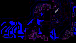
so far I've created the vector graphics
- layer for the photo
- layer for the holes/vias
- layer for the components
- layer for the traces
- layer for the pads
- layer for the bridges

It's partially a two layers because there are some bridges on the top.

To do:
to finish the bottom layer, check for errors, I need to go back to the physical board because some traces are tricky
add the parts name
add the resistor ohm, capacitors farads, IC names, ...
then add the bridges on top

I'm not desoldering the parts of my AB, not yet.. I still hope to be able to fix it, but it there is a donor I could do a better job by scanning the board instead of taking pictured, it is impossible to remove perspective and have everything in focus

I'm learning by doing ...

see below, it's a scree capture
1673302370681.png
 
Last edited:

ironborn65

Well-known member
Thanks, I later realised how damn complex it is but I'm willing to keep going.
I'm at the point where I'm considering to remove the components to measure the values, some are damn small, especially SMD capacitors, I can not read the values. Some are unreadable because too tight to each others. If I had done this before I could have scanned the tracks with a scanner, it's too late now to comply.
The dxf is here https://github.com/pferronato/MacCCAB

I was wondering about the licence though, how has @Bolle dealt with it?
 

ironborn65

Well-known member
more details, I need to remove the cover of the color/video trimmers
 

Attachments

  • Mac CC reverse AB PCB.png
    1.2 MB · Views: 14

joshc

Well-known member
I'm at the point where I'm considering to remove the components to measure the values, some are damn small, especially SMD capacitors, I can not read the values.
Solder them to something where it will be easier to attach a clip/probe so you can read them.

Even small components have markings that indicate their value, sometimes.
A lot of the small ones will probably have similar/the same values.

This is indeed a lot of work, but making a start is probably the hardest bit and you've already done that. Keen to see how it progresses.
 

ironborn65

Well-known member
ok, here I'm out of my comfort zone, assuming there is a zone where I'm comfortable in.

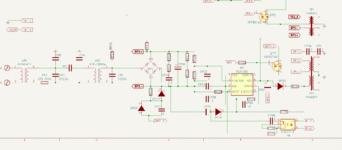
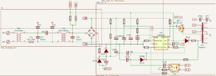
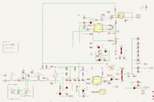
This is my first attempt to use KiCad, this is the partial and incomplete section of the switching, the high energy area. Given the hurdles I think I'll not do the rest, maybe some of the low energy area.
I'm often going back and forth from Kicad schematics <-->2D Cad <--> the real thing.
I need now to use the microscope for getting the readings from the SMD, I need to identify the parts on-line, and add to the list I'm maintaining.
I still find errors in my 2D when I draw the schematics, sometimes it does not make sense and I need to go back to the 2D.
My background in electronics goes back about 35 years and I never practised it, so I'm not able to find inconsistency in the schematics that ends up. In addition I'm learning KiCad while doing, so I'm slow and probably I'm not using it right, even if some basic tutorials on YouTube do help.
I did not find the symbol for the TDA4605 so I created one, but I do not know how correct it is.
In the same way I did not find the IRFBC40, so I created one from a MOSFET N-type that should be quite ok, so it means it's wrong.
I find diodes, but I can not tell if they are a zener, I find a transistor but I can not tell the exact type ...

I'd like to know if someone is willing to contribute to this project, I can keep digging the reali thing but I'm struggling with the schematics

1675294035933.png
 

ironborn65

Well-known member
FYI
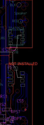
You might all know already, but the Color Classic was designed to be stereo.
I'm wondering ... if the TDA7052B is properly installed with related passive components, would the software work?
From which version of the System is the stereo audio supported?
How can the software detect there is the second channel?

PF

1675927914325.png
 
Top