• Updated 2023-07-12: Hello, Guest! Welcome back, and be sure to check out this follow-up post about our outage a week or so ago.

Carrera040 Info / Hacking Thread

GeekDot

Well-known member
Hey Gang,

Thanks @nickpunt, @trag and @Trash80toHP_Mini for your motivating comments. This helps to keep on writing... crazy what I knew back then and already was about to forget (suffering from "project-ADHD"  :grin: ).
So good to have a "code refresh" while documenting all this in more detail.

That said, prepare for some serious brain-tease (if your brain hasn't already imploded :lol: ) in the just posted part 2hhttp://www.geekdot.com/carrera-in-se-30-code-part-2/
Because I don't want to clutter this thread by upcoming "Hey, new post published!" comments, just follow me on Twitter to get pings about new posts: https://twitter.com/geek_dot 


nickpunt

Well-known member
This is fascinating stuff @GeekDot! You're right about the brain implosion, machine code like this is beyond me. I enjoy reading comments in code though, its like a real time way of seeing your work & thought process. Pretty fascinating how each different machine it supports has special nuances & features, hopefully the overlap of code handling non-32bit clean, ram-based video, and pds can be cobbled together :)  Good luck!


GeekDot

Well-known member
Another quick update:
It's getting clearer every day that little SE/30 and Lady Carrera have an hardware "issue" within their relationship (current status: It's complicated)...

Because the INIT code gets quite far (beyond the 68040 init routine) every 10th-15th try it simply can't be just the driver. There must be some communication/timing issue... 

That said, my logic analyzer just got additional 16 channels (totalling 32) giving me a broader look into what's happening.

Because it's always good to know how others solve(d) the same problem/task, I also started to disassemble the Daystar Turbo 040 ROM.... and at about 4000 lines of code I got caught red-handed  :lol:

66e5ed42f816c70f9089e49addc9ba9a.jpeg.0f852a0e27d175faa901911fa0020436.jpeg


BTW: The Turbo 040 (Rev 1 to 3) looks very much like a by-the-book implementation of what is written in section 7 of the "MC68040 DESIGNER'S HANDBOOK", which is good for a better overall understanding.

 
Last edited by a moderator:

Trash80toHP_Mini

NIGHT STALKER
Thanks for bumping this one, I was looking for a HiRes Pic of the DayStar version and your pic of the Sonnet version in the IP will do. There goes my SE/30 TTL vs. CMOS theory. :-/   But then again, if timings are the issue, there's high speed and then there's HIGH speed logic.

@joethezombie I'm still wondering if board rework yielding faster response from the bus driver/buffer ICs on either side of the SE/30 PDS might help? Accelerators that work fine in the IIci, but are SE/30 hostile might feel more cozy and warm in the SE/30 with snappier 74HCT logic going clickety-clicker? The IIci has a mix of TTL type 74LS Logic and faster CMOS logic of the 74HC series. Not familiar at all with the 74F series, I'm guessing it's a bit slower than 74HCT, but I'm usually one clue short on this stuff  .  .  .  at best. :mellow:

74F573

74HC(T)573


Last edited by a moderator:

Trash80toHP_Mini

NIGHT STALKER
Went back to IP/square one for a reset:

Dang, got things all confuzzled between DayStar and MicroMac 040 cards.  [:I]   Sounds like these suckers changed hands in every case? Did Sonnet wind up with one or the other? Interesting that there's no active component to be seen on the MicroMac Adapter for the IIsi.

View attachment 21545

Finally, not to put a damper on the efforts, but I feel this is going to be a long shot.  I mean, wouldn't MicroMac have made an SE/30 adapter to increase sales of this product?  They made them for the IIsi, IIx, and IIcx, so with the SE/30 mysteriously missing I can only surmise that there is some technical limitation we're going to bump into.  Unless of course, the omission is due to the sealed up nature of the compacts, and MicroMac didn't want to support end users in that endeavor.
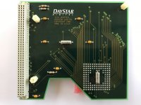
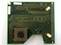
HRMMM? Forgot about this tidbit. Now I wonder if I might be somewhere on the same continent as the track to a solution to this particular conundrum? It seems like adapters for the IIx/IIcx contemporaries of the SE/30 were direct, unbuffered CPU Socket connection interfaces. Got pics of them? No timing lag from PDS buffering imposed on those two adaptations, that now stands out like a sore thumb to me, but I've not been particularly rational this past week. :blink:

edit: trying the Carrera 040 using a IIx or IIcx adapter in a socketed SE/30 comes to mind here. Does testing for function in that configuration sound like it might yield usable info?

 
Last edited by a moderator:

Trash80toHP_Mini

NIGHT STALKER
One more thought: The socket of the IIx and IIcx run at the same 16MHz clock as the SE/30's, but timings may be right on the edge for supporting such a slow bus as compared to the 25MHz bus of the IIci and 20MHz bus of the later IIsi. Wondering if buffering trows the equation just far enough off that the SE/30 was unsupportable. I have no clue as to possible efficacy of rework substitution of 74HCT buffering on one or both sides of the SE/30 PDS, whether it is in fact appreciably more responsive than 74F logic or if  this makes absolutely no sense theoretically. @Bolle whatcha think?

I'll pipe down now. :mellow:

 
Last edited by a moderator:

nickpunt

Well-known member
Odd, I've never seen that variant of the Carrera 040 IIsi adapter. Both of mine (one which came with DiiMo IIsi and other with Carrera 040) have a GAL on them, I assume that one in your picture must have it on the other side. You're right that their IIcx adapter has none at all.

View attachment 11980View attachment 11981

IMG_7019.jpeg

IMG_7026.jpg

 
Last edited by a moderator:

GeekDot

Well-known member
One more thought: The socket of the IIx and IIcx run at the same 16MHz clock as the SE/30's, but timings may be right on the edge for supporting such a slow bus as compared to the 25MHz bus of the IIci and 20MHz bus of the later IIsi. Wondering if buffering trows the equation just far enough off that the SE/30 was unsupportable. I have no clue as to possible efficacy of rework substitution of 74HCT buffering on one or both sides of the SE/30 PDS, whether it is in fact appreciably more responsive than 74F logic or if  this makes absolutely no sense theoretically. @Bolle whatcha think?

I'll pipe down now. :mellow:
Discussed this clocking "suspicion" with Bolle already (We're quite busy behind the scenes ;-)).

I traced the CPUclk (SE/30: 15.6672MHz) coming from the PDS slot to both FPGAs 'TclkIn' pins. Also, the 040s 33.3Mhz clock is fed in there. So my initial (stupid) WAG was, that these two clock-domains used in the FPGA VHDL/Verilog might get into some troubles (Given the FPGAs have to do the dynamic bus-sizing translation between 030 and 040). This would lead to different clocking-ratios:

  • Mac IIci    ~x1,25
  • Mac IIsi    x1.6
  • SE/30       ~x2.10
Who knows how clever their state-machines were designed.... but then it stroke me: Dang! The II[c]x has the very same clocking and these were supported by direct-to-socket adapters. 

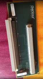
And if my eyes aren't betraying me, the clk-pin on @nickpunts adapter is going straight to A38 on the PDS slot. That said, Nick, it would be interesting to know where A3 (/BUSCLK) is connected to on your adapter...

Next up was the load being put on the clock-signal. I have the short version of @Bolles adapter, sitting on the NIC which also lives off the clock-signal, but "Designing Cards and Drivers..." has the answer:

  • SE/30 - Drive: 40 uA /0.4 mA, 30 pF
  • IIci - Drive: 10 uA/0,1mA, 15 pF
This means litte SE/30 has more ooomp to the CLK signal than his bigger cousin.

So my current "hot trace of the week(tm)" is timing - i.e comparing different runs with my logic analyzer etc. - also I think I won't get around building a 1:1 PDS-interposer to eavesdrop my IIci while smoozing with the Carrera. 
 

Trash80toHP_Mini

NIGHT STALKER
Discussed this clocking "suspicion" with Bolle already (We're quite busy behind the scenes ;-)).
Figured he'd be in on this. [:)]

I traced the CPUclk (SE/30: 15.6672MHz) coming from the PDS slot to both FPGAs 'TclkIn' pins. Also, the 040s 33.3Mhz clock is fed in there. So my initial (stupid) WAG was, that these two clock-domains used in the FPGA VHDL/Verilog might get into some troubles (Given the FPGAs have to do the dynamic bus-sizing translation between 030 and 040). This would lead to different clocking-ratios:

  • Mac IIci    ~x1,25
  • Mac IIsi    x1.6
  • SE/30       ~x2.10
Like a question, a WAG is not stupid by definition. A WAG can be silly, misinformed, way out in left field or outlandishly out side the box  For a question, the stupid one goes unasked as WAG not floated. I think there's something about incandescent light bulb development loosely related to that. [;)]

Assuming the clock ratios of IIx and IIcx are identical to SE/30, it's the delay propagated in buffering the rest SE/30 PDS that got me going. That's straight from Bolle's comments about adding an additional layer of buffering to support a second passthru slot for third card on the very adapter you're using. I've been sitting on a WAG about inadequate bus driving being the culprit in the wonkiness of his SE/30 megastack. The Socketed board vs. the rest of his boards would be the reason for the other thread I started about this, but the wrong 040 board is in the title of that tangent, oh well.

Who knows how clever their state-machines were designed.... but then it stroke me: Dang! The II[c]x has the very same clocking and these were supported by direct-to-socket adapters. 

And if my eyes aren't betraying me, the clk-pin on @nickpunts adapter is going straight to A38 on the PDS slot. That said, Nick, it would be interesting to know where A3 (/BUSCLK) is connected to on your adapter...

Next up was the load being put on the clock-signal. I have the short version of @Bolles adapter, sitting on the NIC which also lives off the clock-signal, but "Designing Cards and Drivers..." has the answer:

  • SE/30 - Drive: 40 uA /0.4 mA, 30 pF
  • IIci - Drive: 10 uA/0,1mA, 15 pF
This means litte SE/30 has more ooomp to the CLK signal than his bigger cousin.
Makes sense, that oomph is there to drive an expansion bus spec limited to just two TTL inputs while the IIci Cache Slot was designed to support just one. The IIsi PDS would be the same spec, but for the clock ratio disparity.

So my current "hot trace of the week(tm)" is timing - i.e comparing different runs with my logic analyzer etc. - also I think I won't get around building a 1:1 PDS-interposer to eavesdrop my IIci while smoozing with the Carrera. 
In WAG mode, methinks the quality of your schmoozing time would increase dramatically by building an interposer. But  on built for the 030 socket interface and gated for three states: straight thru, 74F573 type and 74HC(T)573 type buffered latches or the equivalent of whatever buffer IC is used to drive the PDS of the SE/30. That would be the bottleneck for SE/30 adaptation the way I see it in this table:

IIci - are the Cache Slot signals buffered, don't think so IIRC? @ ~x1,25 multiplier = functional = Baseline design spec of Carrera 040 et al.

|

IIsi - PDS Bus signals (straight thru on Carrera specific IIsi adapter) buffered @ ~x?.?? multiplier = functional*****

|

SE/30 - PDS Bus signals buffered @ ~x2.10 multiplier = non-functional

|

II(c)x - direct socket connection signals straight thru @ ~x2.10 multiplier = functional, but suspected edge case for timing*****

***** if you build an interposer, some interesting tests become possible, but after doing a feasibility study:

View attachment 21545

View attachment 21546

Nope, no GAL on this version, nick. IIci adaptation is built into the Carrera's bits and interposing joe's adapter between II(c)x adapter and Carrera in a II(c)x would not cause loss of function under my premise.

View attachment 11980

I suspect that interposing your PowerCache adapter with IIci conversion in that GAL would cause failure due to timing issues propagated in the GAL.

Outlandish WAG here is that the delays propagated by the GAL on Bolle's PowerCache adapter that you've been using on top of inherent buffering delay of the SE/30 PDS would be the root cause of your timing issues at the ~x2.10 multiplier.

Dunno what the CMOS logic I found in schematics of IIci and IIsi might do, but there has to be a very good reason for going to the trouble of using 74HC logic that's not TTL compatible in the designs. TTL compatible 74HCT (if available in that time frame?) would have been a seamless way to implement much faster, lower power consumption CMOS logic.

That's my WAG  .  .  .  and I'm still sticking to it. :blink:

 
Last edited by a moderator:

Bolle

Well-known member
So as you can see the Carrera kind of works in the SE/30 after some fiddling but onboard video is broken.

Besides those vertical white bars everything else is rock solid.

To get around the video issue the only way right now is to use a Micron card for internal GS:

View attachment 30066

While digging through the init geekdot kept insisting that we had a hardware timing issue which resulted in the crashes right when the init loads to enable the C040.

I wouldn't believe him at first but he wouldn't stop :-*

When working on the PowerCache I discovered that they have a clock distribution GAL on there that takes the 16MHz clock from the logicboard and distributes it to various other GALs that need this signal.

They implemented a way to shift the phase of the clock signal that gets distributed on the PowerCache depending on how some of the undocumented pins on the cache slot are either tied to ground or left floating (which pulls them up internally on the GAL)

On the official Daystar adapters those pins are configured for each machine type. This results in the 16MHz clock signal being phase shifted using feedbacks in the GAL just a little bit more or less for each machine. (they also have an external feedback circuit right next to that clock distribution GAL but they did not populate it with any components)

This made me think that certain machines seem to have slightly different timing requirements that need to be accommodated on the accelerator.

With that in mind I tried what happens when I shift the phase of that clock on my own before it even enters the accelerator. On the PowerCache it did not seem to make any difference (in the SE/30 at least - didn't try any other machines)

When I inverted the clock signal the Turbo 040 would suddenly work if I stuck my adapter on top of a MacCon which wasn't working very well (if at all) before. Even two PDS cards would work together nicely with the Turbo 040 that way.

Surprised by those findings I modified my Carrera adapter to do a 180° phase shift on the 16MHz clock as well and it booted up right away, loading the init without crashing and was running rock solid. (the init still needs WiW or patching of the IDs to load)

Right now we are not sure where the onboard video issues originate. QuickDraw was a suspect but we did not totally rule out that it still might be a timing issue of some sort after all.

Trying to find out if fine-tuning the phase of the 16MHz clock gets us somewhere is the next thing on the list.


GeekDot

Well-known member
While digging through the init geekdot kept insisting that we had a hardware timing issue which resulted in the crashes right when the init loads to enable the C040.

I wouldn't believe him at first but he wouldn't stop :-*
LOL - love you too, bro! 

Right now we are not sure where the onboard video issues originate. QuickDraw was a suspect but we did not totally rule out that it still might be a timing issue of some sort after all.
...and QuickDraw just uses, whatever method the driver offers to set pixels. So what the heck, I've disassembled the SE/30 driver-ROM, too.

See the disassembly here https://github.com/axelmuhr/Carrera040/blob/master/se30vrom.asm - the most of it is sRecords and the dev-team rightfully celebrating themselfes  ;)

Having a look at line #531 you can see how it's done: A simple move.l to the screenbase at 0xFEE08040. So 32bits are written "at once" and there's no simple software explanation why there's a 'whiteout' in the 3 byte resulting in those stripes you can see 3 posts above this. It has to be hardware timing...

Trying to find out if fine-tuning the phase of the 16MHz clock gets us somewhere is the next thing on the list.
I tried delaying the clock using a 74LS31...


Delay


Pins


Result


6ns Inverted (NANDed)


(5 NAND 6) -> 7


Stripes plus Buserror


12ns


(5 NAND 6) -> 7 ->(10 NAND 11) -> 9


Hangs (like 1:1 clock)


23-32ns Inverted


1 -> 2


Stripes (roughly equals NOT)


45-48ns


3 -> 4


Stripes


51-54ns Inverted


3 -> 4 -> (5 NAND 6) -> 7


Hangs (like 1:1 clock)


So effectively only delays of ~23-48ns result in a kind of successful boot - both are close to a 50% clock-shift (plus propagation-delay) of the 63.82ns duty-cycle of the  15,6672MHz from C16M.

This is, where I'm a bit lost ATM... are we looking at a phase-shift issue here? Or do we need to stretch timing vs. just delaying it? I wish I were an educated engineer... ;-)


Bolle

Well-known member
Boom... got rid of the stripes.

xULCIIG.jpg.d7129119d06a87690e3692985c4278fe.jpg


Notice the funny prototype adapter:

pavhOK5.jpg.8a1ff73d171d745a972b34e0476bb47c.jpg


QuZkG43.jpg.a72175de5dca59560ad342e3f8cc5684.jpg


This won't support any additional PDS cards at the moment but adding the necessary decoding logic won't be hard.

 
Last edited by a moderator:

AlpineRaven

Well-known member
Wow thats good news... good on ya - Ive got one of those CPU cards and very keen to use one day! If someone is able to make an PDS adapter.
Cheers

AP

 
Top