• Updated 2023-07-12: Hello, Guest! Welcome back, and be sure to check out this follow-up post about our outage a week or so ago.

601 processor replacement experiments

Trash80toHP_Mini

NIGHT STALKER
Curious, I'll have dive back into the PDF docs once again it seems.

It's looking like my theoretical interstitial QFP to BGA adapter could be the way to go. The cache deprived 1400/117MHz processor card would be the best candidate as there would be no slow L2 cache complications. Only two tiny caps stand in a 23mm wide pathway between another two pairs of caps into the "cache overhang" space of the higher end processor cards with cache. A pair of holes in the adapter PCB takes care of that clearance problem with plenty of area left on the multiple layers for the lines required for support components/voltage doohickeys.

The only complication would be that such an extension buries the QFP pads on that side of the adapter. Such may not be a problem as higher temperature hot air installation would be possible. There are ZERO active components on the processor card. Every component is a silk screen layer identified cap, resistor or resistor pack save a curious boxy two connection somethingorother. I'll need to buz the connections, WAG would be a voltage converter?

This brings up a second approach that's nontrivial at best and outright insane at worst. The 117MHz card appears to be done in four layers and amounts to an interboard connectors to QFP adapter with a workable sprinkling of power leveling and termination(?) glue on board. Caffeine deprived morning musing today would be to design a new processor card for the BGA G4 of choice with cache on die instead of the interstitial adapter. As in the statement above, the cantilevered "cache extension" provides more than adequate PCB real estate for support components.

If the high 32 bits of a 64bit CPU were terminated would that suffice to use such a beast on a 32bit bus? We're talking shades of the LC's lamed 32bit 68020 running on a 16bit bus. A two generation CPU upgrade with cache on die at a HIGH bus multiplier on the 1400's 32bit bus hardly qualifies as "laming." [}:)]

I hope this makes some kind of sense? :blink:

*** I'm beginning to wonder if Wegener employed an interstitial BGA to BGA adapter for theig Pismo G4 upgrades?

edit: designing a new processor card with CPU specific support components would almost have to be a more practical approach (and far more efficient) than an interstitial adapter board. BGA to board interconnects on either side has to be easier than the spaghetti mess of BGA to QFP pads on all four sides. I wonder if the interboard connectors are still available? Donor card harvest/reinstallation on the G4 adapter ought to be easy enough, no?

 
Last edited by a moderator:

Trash80toHP_Mini

NIGHT STALKER
I've seen a couple references to people swapping a 7400 onto a 750-based Pismo CPU card but I'm not sure how they do it. I haven't compared the 7400's pin-out to the 750's because I simply assumed they were different (IIRC the 7400 has a wider address and/or data bus than the 750). It's possible that the 7400 and 750 share the same or close enough pin-out to share a similar mount but at this point I can only speculate. If they are interchangeable, I know you won't be able to do this with any chips other than the 750/750L and the 7400 or 7410; the later chips are most definitely incompatible.
I found a spec sheet on the 7410 and it's out of the running, the PLL settings/multiplier table lists no support for a 33MHz system bus.

The 7400 multipliers only go up to 8x in the spec in one place, but the PLL settings table also shows 9x, still too slow to be in contention unless a 300MHz G4 stomps a 466MHz G3?

@trag  Quest lists the PPC750FX-GB0132T as available, but I see no spec for the max processor speed? Is that the 800MHz part you listed? The PPC750L-GB450A2 is a bit slower than my Sonnet 466/1MB. Earlier you said:

They have some (7) 750FX at  800 MHz for $32.50.  That's pretty good.   292 pin BGA (21mm X 21mm).   The 750FX has up to a 20X bus multiplier.

Anyone know how the 750GL differs from the 750GX?    They have 81 750GL for $34.50 - $39.    Same package as the 750FX and also up to 20X multiplier.   The GL has a 1MB L2 cache like the GX...
The 292 pin versions appear to have cache lines broken out, whereas the 256 pin (740 and 750CX?) CPUs don't as I recall from reading earlier tonight. If the CPUs you listed have 1MB of L2 on die, those cache lines must be for an L3 setup we never saw in a Mac because of the switch to G4? What was the fastest G3 Apple shipped anyway? If I can disable/terminate those L3 lines on a 292 pin package, a G3 with 1MB of on die L2 running on a 20x multiplier at 666MHz would do nicely for the 1400 unless a G4 candidate can be identified. Don't recall, does the on die L2 run on the CPU clock or on a divider?

Found another G3 in stock: PPC750FX_GB1033T_FB1033T but the speed (1033MHz?) would be wasted. 33.3MHz bus x 20 = 666MHz ceiling for a PB1400 CPU and heaven only knows what they'd cost if I'm deciphering the coding correctly? Way beyond my wildest dreams, but with that imaginary L3 implemented one might make a nice GigaHertz L2 Slot Accelerator for the 50MHz bus of the TAM. [}:)]

OK, well past time for an egg nog! [:)]

 
Last edited by a moderator:

CC_333

Well-known member
Well, I don't have much to add here, but my understanding is that one of the few significant advantages the G4 has over the G3 is the former's AltiVec engine that can boost certain things like Photoshop plugins and I believe Mac OS X makes use of it, particularly in Tiger. The G4 can also support multiprocessing (SMP) (irrelevant here, but still of potential interest in general), whereas the G3, oddly, cannot.

c


Franklinstein

Well-known member
Curious, I'll have dive back into the PDF docs once again it seems.

It's looking like my theoretical interstitial QFP to BGA adapter could be the way to go. The cache deprived 1400/117MHz processor card would be the best candidate as there would be no slow L2 cache complications. Only two tiny caps stand in a 23mm wide pathway between another two pairs of caps into the "cache overhang" space of the higher end processor cards with cache. A pair of holes in the adapter PCB takes care of that clearance problem with plenty of area left on the multiple layers for the lines required for support components/voltage doohickeys.

The only complication would be that such an extension buries the QFP pads on that side of the adapter. Such may not be a problem as higher temperature hot air installation would be possible. There are ZERO active components on the processor card. Every component is a silk screen layer identified cap, resistor or resistor pack save a curious boxy two connection somethingorother. I'll need to buz the connections, WAG would be a voltage converter?

This brings up a second approach that's nontrivial at best and outright insane at worst. The 117MHz card appears to be done in four layers and amounts to an interboard connectors to QFP adapter with a workable sprinkling of power leveling and termination(?) glue on board. Caffeine deprived morning musing today would be to design a new processor card for the BGA G4 of choice with cache on die instead of the interstitial adapter. As in the statement above, the cantilevered "cache extension" provides more than adequate PCB real estate for support components.

If the high 32 bits of a 64bit CPU were terminated would that suffice to use such a beast on a 32bit bus? We're talking shades of the LC's lamed 32bit 68020 running on a 16bit bus. A two generation CPU upgrade with cache on die at a HIGH bus multiplier on the 1400's 32bit bus hardly qualifies as "laming." [}:)]

I hope this makes some kind of sense? :blink:

*** I'm beginning to wonder if Wegener employed an interstitial BGA to BGA adapter for theig Pismo G4 upgrades?

edit: designing a new processor card with CPU specific support components would almost have to be a more practical approach (and far more efficient) than an interstitial adapter board. BGA to board interconnects on either side has to be easier than the spaghetti mess of BGA to QFP pads on all four sides. I wonder if the interboard connectors are still available? Donor card harvest/reinstallation on the G4 adapter ought to be easy enough, no?
The 603 was designed to allow selection of either 32 or 64 external data lines; the 7400 is possibly also configurable to use fewer data lines, but I haven't read the manual. In the 1400 (and its progenitors, the PB 5300/2300) the 603e lives on a 32-bit data bus. Since 750 upgrades work in the 1400 (and are derived from the 603) it stands to reason that the 750 is also configurable to operate with a 32-bit data bus. 

Just because something doesn't officially support a given bus speed doesn't mean it won't. For example, the 37.5MHz bus in the 52/62xx computers is an unsupported configuration for the 603; the 75MHz part was supposed to be operated at 3x on a 25MHz bus (the original 603 does not support half multipliers). Officially supported bus speeds for the 603 are 16, 20, 25, 33, 40, 50, 60, and 66MHz. It's entirely possible the 7440 will run on a 33MHz bus, but depending on its max multiplier, I don't see it going much over 667MHz (20x bus speed). 

I know that a good number of the PowerBook G3 upgrade cards were custom built with Flash chips instead of Apple-produced ROM chips, so they're out there. I don't know how they got around that. Maybe because they were designed for use exclusively in Apple products? Maybe they operated exclusively on trade-ins? Maybe they paid a royalty? 


Franklinstein

Well-known member
I found a spec sheet on the 7410 and it's out of the running, the PLL settings/multiplier table lists no support for a 33MHz system bus.

The 7400 multipliers only go up to 8x in the spec in one place, but the PLL settings table also shows 9x, still too slow to be in contention unless a 300MHz G4 stomps a 466MHz G3?

@trag  Quest lists the PPC750FX-GB0132T as available, but I see no spec for the max processor speed? Is that the 800MHz part you listed? The PPC750L-GB450A2 is a bit slower than my Sonnet 466/1MB. Earlier you said:

The 292 pin versions appear to have cache lines broken out, whereas the 256 pin (740 and 750CX?) CPUs don't as I recall from reading earlier tonight. If the CPUs you listed have 1MB of L2 on die, those cache lines must be for an L3 setup we never saw in a Mac because of the switch to G4? What was the fastest G3 Apple shipped anyway? If I can disable/terminate those L3 lines on a 292 pin package, a G3 with 1MB of on die L2 running on a 20x multiplier at 666MHz would do nicely for the 1400 unless a G4 candidate can be identified. Don't recall, does the on die L2 run on the CPU clock or on a divider?

Found another G3 in stock: PPC750FX_GB1033T_FB1033T but the speed (1033MHz?) would be wasted. 33.3MHz bus x 20 = 666MHz ceiling for a PB1400 CPU and heaven only knows what they'd cost if I'm deciphering the coding correctly? Way beyond my wildest dreams, but with that imaginary L3 implemented one might make a nice GigaHertz L2 Slot Accelerator for the 50MHz bus of the TAM. [}:)]

OK, well past time for an egg nog! [:)]
I'm out of nog  :(

I put my comment about the unsupported bus speeds in the wrong section so see above.

The 750GX was originally available at 1.2GHz or better with a maximum 200MHz bus speed, something Apple never implemented in a G3 (I don't think they went over 100MHz). I think the 750FX also could drive a 200MHz bus in some versions and it was available up to at least 1GHz. 

No 750 variant ever supported L3 cache.

The 740 does not support a backside L2 cache, but assuming it is 100% compatible with the 603e, it will support a bus-level L2 cache. The 750 has an integrated L2 cache controller to support a variable high-speed backside L2 cache, though the extra pins required make it no longer pin-compatible with the 603e. The 750CX brought the cache on-die (256k at full speed) so it no longer had need of the L2 cache pins of the original 750, yet it was also not pin-compatible with the 750 or 603e. The 750FX was a major improvement including new power-saving features, more L2 cache (512k), and higher clock and bus speeds; it was also not pin-compatible with any of its predecessors. The 750GX was a minor enhancement of the FX consisting mostly of higher clock speeds and another doubling of the L2 cache (to 1MB); it is pin-compatible with the 750FX.

The fastest Macs Apple shipped with G3s were: B&W G3 at 450MHz (750L), PowerBook G3 Pismo at 500MHz (750L), iMac SE at 700MHz (750CX), and the opaque white iBook G3 at 900MHz (750FX).

I would personally enjoy a 1GHz L2-style 750GX upgrade, if we're thinking about taking orders. An 800MHz variant would probably be better value (the law of diminishing returns and all) but if we're going to the trouble, may as well go all the way.


Franklinstein

Well-known member
Well, I don't have much to add here, but my understanding is that one of the few significant advantages the G4 has over the G3 is the former's AltiVec engine that can boost certain things like Photoshop plugins and I believe Mac OS X makes use of it, particularly in Tiger. The G4 can also support multiprocessing (SMP) (irrelevant here, but still of potential interest in general), whereas the G3, oddly, cannot.
AltiVec, additional and/or wider internal sections (decoders, ALUs, etc), and full MESI support for multiprocessing were the 7400's advantages over the 750. Like the 603, the 750 only had partial multi-processing support (only MEI instead of the full MESI suite), so it was unsuitable for such applications.

Clock-for-clock the 7400 is faster than the 750, but not by much; unless an app is AltiVec-enabled, most tasks aren't noticeably faster, while the 7400's greater power consumption and heat output generally are. Unless you're doing nothing but A/V work (PhotoShop, FCP, iMovie, iTunes, whatever else may have AltiVec extensions) there's no real point to a G4 upgrade for Classic Mac OS, especially since the all-important AltiVec support requires OS 9 or later.


Franklinstein

Well-known member
Good news: I finally looked up the specs for the 750 and the 7400, and they're basically pin compatible: they're both 360-pin BGA devices and all but 10 pins are the same. The 10 different pins may be inconsequential, and it would appear that they are, given that people have done swaps without apparent issue. The only concern would be boot-level software support, if it's required. A closer inspection of those Sonnet G4 upgrades suggests that they have Apple ROMs and additional Flash devices which may hold patches to support the new 7400, but then there's a seller on Yahoo! that advertises a simple swap of the processors on a Pismo card. Maybe a patch disk is included? I dunno.


Trash80toHP_Mini

NIGHT STALKER
Upgrading PCI PowerMac 5/6x00 L2 upgrades (was) Sonnet Clocker II - gotta dig up the Sonner Clocker II thread.

_____  Bolle joined that thread with a link to info on his work from a year ago in 's @max1zzz's work from two years ago

iMac G3 (Rev A -> C) G4 CPU Upgrade

_______________  I'll find all the ProcSwap threads eventually, help would be appreciated.

Lets see, I'm only interested in machines that run OS9 on the 603e at this point, so:

I settled on a redesign of the 1400's 117 MHz processor card for simplicity's sake. LOL!

____  building a BGA to CPU card's board interconnect is the most flexible experiment

________  no interstertil adapter experimentation involved

____  No cache problems to crop up as in max's thread

____  It's a driver free swap of the CPU board

________  as it's currently proposed anyway

____  there shouldn't be any ROM complications, it'll "just work" or not as the case may be

________  only signal compatibility at boot would be required as I see it anyway

No OSX means ALTIVEC's not a requirement

____no sane person does supported graphics work on 603e

____a higher multiplier (20x) on a G3 trumps a lower multiplier G4 that won't crank to 666MHZ on a 33.3MHz bus

 
Last edited by a moderator:

Trash80toHP_Mini

NIGHT STALKER
Ran out of edit time so please excuse the spelling and worse than usual stream of incoherence above. Didn't get a chance to say thanks much for your help and research, Franklinstein. @trag too of course.

@Cory5412 it's probably about time to break my ridiculous 603e tangent off this 601 topic and into its own hacks thread like the last one. Maybe something like "1400 Processor Card - New Build Proposal?"


Trash80toHP_Mini

NIGHT STALKER
:lol:  Shutting my brain down in the shower works even after caffeine has kicked in. Just realized the proposed 1400 processor card development amounts to a BGA to BGA interstitial adapter PCB prototype on much a larger scale. QFP to BGA can wait, a BGA to BGA CPU upgrade on a 50MHz bus could be very interesting indeed.

 
Last edited by a moderator:

trag

Well-known member
I saw the summons just now, but Franklinstein pretty much wrote what I would have said, and more.  In summary:

1)  Bus speed doesn't matter, except for calculating potential CPU speeds.    All the processors you're looking at will run fine at the slow bus speeds that the Apple machines use.

2)  There are no L3 caches and no external cache support on the 750CX, FX and GX.    The 750 had support for an L2 cache.  If the L2 cache is internal, then there are no external Cache signal pins.

3)  As you concluded, bus multiplier is very important.    The early PPC750 only went up to 8X.  The 750L raised that to 10X.   The early G4/7400 only went up to 9X.    Later G4 models had higher multipliers, but I don't think that the later models are pin compatible with the PPC750.

4)  Only the 740 was pin compatible with the 603.   All other choices require a new board.

4)   If you're considering a brand new board, then later G4 chips are back on the table with higher multipliers, on-board cache, and potentially, external L3 cache.    But, Cost.


Trash80toHP_Mini

NIGHT STALKER
Thanks much for the feedback. If I take anything like this into AI for hand routing playtime it's definitely gonna be a brand new CPU board design for the 1400. That processor card is by far the handiest testbed for this kinda crap in the 603e menagerie. Have I mentioned I have close to a two foot stack of the damn things and one arriving mid-week with my fourth G3 card on board? :lol:

Cost concerns you brought up had me looking up the CPU in my PartsBookAl/1GHz at work. It's the 7447A, its 21x multiplier takes it to 693MHz on a 33MHz bus and that'd be 1050MHz if it translates to an L2 board someone else might take on at some point. Same is true of an interstitial adaptation for a mobo ProcSwap that might be marginally less insane to take on. That route would certainly be a lot more flexible in terms of machines supported.

Signal to signal, 7447A <-> 603e looks like a hot mess and I've not even gotten down to GND in the alphabeticals. So I looked up iBooks on everymac thinking about the 900MHz G3s you mentioned, Franklinstein. But I found 800MHz, 933MHz and 1.0GHz G4 iBook models all using the 7457.  Haven't got to signal comparisons yet, but the chip's shit hot! Maybe that'd be cool shit? Must be a lower power/cooler running CPU because the multiplier tops out at 28x, which would be 933MHz on the 1400's 33MHz bus. [:D]

So, of course the signal compatibility cannot possibly work out. ::)

 
Last edited by a moderator:

Franklinstein

Well-known member
At some point (I think the 7440/7450) the G4 no longer supported the 60x bus, only the MaxBus. The later chips could be run on a 60x-based machine but they required a bunch of adapter chips, which explains why there are very few >500MHz G4 upgrades for anything other than PCI Power Macs or UniNorth-based G4s. I did recently acquire a 700MHz Crescendo ZIF upgrade and it's huge, easily a 6" long card, with four QFPs and one BGA chip on it (in addition to the processor and two L3 cache chips).

All of the 750 variants support the 60x bus, so there are no bus-related problems with using a 750GX on an originally 603-based machine.


Paralel

Well-known member
For whatever its worth, Newer Technologies was able to essentially drop in a 740 G3 in place of a 603e processor on one of their blackbird CPU daughterboards because they are apparently fully pin-compatible, However, by the time their 740 G3 prototypes were completed, the interfaces for the CPU daughterboards were no longer being produced, so it was dead in the water.

Also, apparently in Japan, a guy was able to take a Newer Technology NuPower 167 Mhz CPU daughtercard, pop off the 603e, drop a 740 G3 in its place, and it worked without any difficulty.

From what I can tell, the PPC740L would be a drop-in replacement for the 603e.

Being a blackbird fan, I would like to see a 740 G3 run on a blackbird.

 
Last edited by a moderator:

Trash80toHP_Mini

NIGHT STALKER
That Newer ProcSwap is great news. Not a practical approach for a first attempt though. Got sidetracked into the SE/30 morass for a bit last night right after work. An attitude adjustment later, I sat down to this and decided CPU availability was more relaxing than doing a block diagram of all transplants reported to have been successful. Dumb, idea every roll of the G4 dice came up came up snakeyes. That frustration sent me over to the G3 slot machine. There I hit for a nice jackpot. The cup ran over with 32,324 tokens PPC750FX-GB1033T PPC750FX BGA They're more expensive than @trag 's finds, but I don't foresee running out of a CPU similar to the 750LX used in Apple's iBook series from mid-1992 up to the G4 series.

666MHz is an appropriately devilish challenger for the Crescendo PB G3/466/1M in Beater, my grizzled 1400c RoadWarrior veteran. [}:)]

 
Last edited by a moderator:

Trash80toHP_Mini

NIGHT STALKER
edit: oopsie! The above should have read "similar to the 750FX used in the iBook G3 series and (possibly the same as?) the CPU in the end of series 900MHz iBook G3.

Original PPC750 was in a 360 pin BGA (25mm X 25mm) with 8X maximum bus multiplier and selectable IO voltages of 3.3V, 2.5V or 1.8V.

PPC750L raised maximum bus multiplier to 10X.   These are the "copper" G3s.  360 pin BGA (25mm X 25mm)  

PPC740L     As above, but in 255 pin BGA (21 mm X 21 MM).    I guess this is the PPC603 compatible package, but not certain.

PPC750CX   Moved L2 cache to on-chip.   256K L2 cache on-chip.   Up to 10X bus multiplier.   256 pin BGA (27mm X 27mm)

PPC750FX   L2 cache increased to 512KB.  up to 20X bus multiplier.   292 pin BGA (21 mm X 21 mm)

PPC750GX, as 750FX except on-chip L2 cache increased to 1 MB
Dunno where a the 466MHz 750 on a 33MHz bus with off chip (backside) L2 on the PCB extension might fall into that chart. EveryMac's timeline data for that accelerator series would be:

Crescendo PB 333MHz 1/5/2000 release date jibes with PPC750L its 10x multiplier/external cache pincount

Crescendo PB 400MHz 7/19/2000 release date implied 12x multiplier breaks the 10x multiplier mold with external cache/pin count?

Crescendo PB 466MHz 2/15/2002 release date implies a 14x multiplier, also with backside L2 cache/pin count?

Release dates of the 750FX CPU and its speed bumps will need to be hashed out. It shows up mid-2002 on the 100MHz bus of the 600MHz iBook and tops out at 900MHz in the 2003 iBooks. That makes me wonder about bus multipliers and Apple's penchant for laming lower end models so as not to cannibalize high end model sales. But that's another, unrelated story/tangent/rabbit hole for someone else to explore.

_____________________________________________________________________________

My original question bringing on this line of research would be my curiosity about performance comparison of 512MB on die (frontside) L2 of the 750FX vs. 1MB external (backside) L2 on whatever the heck CPU is on the 2002 Crescendo PB 466MHz/1M I bought from Sonnet in 2005 to use the free WiFi of this smalltown downtown, NC?

So what should give better performance, 1M clock divided backside L2 or 512K of on die (frontside?) L2?

Bonus question: what the heck does Crescendo G3/PB 333/512k (1M) and 512k, 1 MB (backside) L2 in the EveryMac spec mean?

 
Last edited by a moderator:

Franklinstein

Well-known member
My original question bringing on this line of research would be my curiosity about performance comparison of 512MB on die (frontside) L2 of the 750FX vs. 1MB external (backside) L2 on whatever the heck CPU is on the 2002 Crescendo PB 466MHz/1M I bought from Sonnet in 2005 to use the free WiFi of this smalltown downtown, NC?

So what should give better performance, 1M clock divided backside L2 or 512K of on die (frontside?) L2?

Bonus question: what the heck does Crescendo G3/PB 333/512k (1M) and 512k, 1 MB (backside) L2 in the EveryMac spec mean?
The Crescendo PB 466/1M is most likely using an IBM 750L, the favored copper variant of the late-model 750 chips.

To quote Red Hill Technology, "more cache good; faster cache gooder." External SRAMs were kinda slow, especially as processors ticked up into the GHz range, so while you may be able to stick 2MB of backside cache on something, if it's only running at half processor speed (or less), it doesn't provide any more of a performance benefit than 1MB of on-die cache. In the 466/1M Crescendo, that 1MB of cache isn't running any faster than 2:1, more likely less (at least from stock; I think the control panel let you adjust that but stability wasn't guaranteed in all configurations). While this may be faster than a 750CX (it is 4x greater than the 750CX's 256k of cache), it will be the same as or slower than the 750FX's 512k. Rule of thumb: if a backside cache is </=2x the on-die cache of a comparable processor, the on-die variant will be the same or slightly faster. Especially if we're building new devices, the on-die variant would be preferable because there would be fewer devices to buy and would allow a much simpler PCB layout.

The Crescendo G3/PB 333 was probably available with a choice of 512k or 1MB models, depending on how much you wanted to spend. I'd bet there was a $50~80 difference between the two. The other option is that it was a long-lived product and it was upgraded from 512k to 1MB in later examples, much like the last of their Crescendo G4/PCI cards that used 1GHz+ chips when the slower ones were out of production.


Trash80toHP_Mini

NIGHT STALKER
The Crescendo PB 466/1M is most likely using an IBM 750L, the favored copper variant of the late-model 750 chips.
Thanks for the info, gotta see if I can get the ole' girl up and running to gimme any answer at all about what's under her yellow rubber panties.

To quote Red Hill Technology, "more cache good; faster cache gooder."
That's about what I was guessing, that 32K available CPU count is looking goodest about now.

Keep It Simple Stupid! is my mantra and it doesn't get any more simple than this:

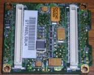
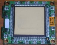
1400-117-ProcCard-001.JPG

What the heck is that black Box?

This one I've already peeled off, but gotta clean it up to read it.

1300-117-ProcCard-000.JPG

Gotta find and get the continuity testing gear together to buzz a cable and then get busy with this little darling unless somebody has any serious reservations to bring up about my FX plans? Tomorrow I'll use the hot air station to pull the connectors off my partially denuded schematic development victim. That could make things a little easier. Connector pinout is the first step for wherever the wind blows this silliness.

PPC750FX-GB1033T PPC750FX BGA does mean 1033MHz CPU, no? 20x multiplier, here we go!

 
Last edited by a moderator:

Trash80toHP_Mini

NIGHT STALKER
603e is a 240 pin package with lots of redundancy of power and ground. Interconnects appear to total 160 pins with what's likely many fewer PWR/GND connections fanned out across the processors legs with load leveling and bypass caps aplenty.

CPU says XPC603EFE117MJ - Moto Logo  .  .  .  and what the heck is that black box with red sides?

 
Top