• Updated 2023-07-12: Hello, Guest! Welcome back, and be sure to check out this follow-up post about our outage a week or so ago.

601 processor replacement experiments

Franklinstein

Well-known member
Since I started diving back into these NuBus models, I was curious if I could replace the 601 chip with faster ones. This is possible, sort of:

The original 601 was built using a single 5v power supply and ran at frequencies between 60 and 80MHz. So yes, it's entirely possible to take a 6100/60 and swap in an 80MHz processor. This isn't really worth it on the 7100, 8100, or 9150, since they already had 80MHz options available; I wouldn't bother unless I had to replace a damaged chip anyway.

The 601v was a mild redesign using a smaller manufacturing process, which allowed it to operate between 100 and 120MHz, and a dual power system: 2.5v and 5v. Unfortunately this new power system made it incompatible with the original 601, precluding its use in anything except the 8100/100 (the 601v-capable 9150 already ran at 120MHz), which could then be stepped to 120MHz if you could find the faster chip.

I haven't yet investigated but I am curious as to whether the original QFP 604 is pin compatible with the 601v. A 604-based 8100 could be an interesting machine.

 

Trash80toHP_Mini

NIGHT STALKER
Now that you mention it, the QFP/BGA CPU rift is a massive PITA when it comes to upgrading processors. Stupid expensive prototyping adapters were once available. Now that four layer boards are so inexpensive I'm toying with a very old notion again.

A PCB adapter with QFP contacts on the bottom for solder mask/hot air installation on the mobo and BGA adaptation contacts on top might be feasible in this day and age? Adapting to signal compatible later generation CPUs with convenient clock multiplier resistor pads next to the BGA CPU's pads could make for some kick ass experimentation.

edit: notion goes all the way back to the ill fated 2300c/G3 thread over on 'fritter. I'm thinking thinner thermal tape on a hot processor. No need for such on the NuBus PPC machines. No cache, but what the heck, you're only looking for faster clocks at this point, no?

 
Last edited by a moderator:

Gorgonops

Moderator
Staff member
Looking at the datasheets for the 604 and 601 it looks like it's a hard no. They're both 304 pin packages but the pin assignments don't match up at all. (Like, literally, the same pin is a voltage supply on one but a ground on the other, and the signals are likewise completely scrambled. It almost looks like they intentionally made them as incompatible as humanly possible.) So at the very minimum you'd need some sort of adapter board.

 
Last edited by a moderator:

Trash80toHP_Mini

NIGHT STALKER
I wish someone would make up a table of signal, if not pin or even package compatible processors for adaptation. Thinking in tables makes my head hurt. :p


Franklinstein

Well-known member
Looking at the datasheets for the 604 and 601 it looks like it's a hard no. They're both 304 pin packages but the pin assignments don't match up at all. (Like, literally, the same pin is a voltage supply on one but a ground on the other, and the signals are likewise completely scrambled. It almost looks like they intentionally made them as incompatible as humanly possible.) So at the very minimum you'd need some sort of adapter board.
Bah. I hadn't got around to comparing those yet and am now sad :(  Not too sad, though; it's just a fun potential for experiment is all. Also useful for honing my SMD rework skills.

I wonder if they also redesigned the 601v to be intentionally disruptive? I am guessing no, since the whole PPC project was in a state of turmoil for the first few years as they fine-tuned the platform. I mean, the PPC 740 is both pin and signal compatible with the BGA 603e so at least if they were being vexatious at first they changed their mind in later years.

As far as using a crazy QFP-to-BGA adapter, I can see how it may be physically possible: build a board with the 304-pin QFP pinout that aligns to whichever chip you're replacing (apparently the 601, 601v, and 604 all have the same number of pins but different pinout) and send the signals to BGA lands that correspond to whichever device you're going to install (604, 603/740, 750, maybe 7400?). The QFP board would be physically large enough to wire and mount a BGA device in its center so it wouldn't be tremendously difficult, except you would probably also need to work out a VRM of some sort to account for the lower voltages used by the newer devices.

Or better yet: send the lines to a ZIF socket! BOOM: instant ZIF-upgradeable NuBus Power Macs, complete with whatever L2 cache is on the ZIF module. GENIUS! Somebody with time and talent should make that happen. I would buy a couple. I mean, a 400MHz G3 6100 (of course I would clock the system bus to 40MHz at the same time)? Super awesome.


Franklinstein

Well-known member
edit: notion goes all the way back to the ill fated 2300c/G3 thread over on 'fritter. I'm thinking thinner thermal tape on a hot processor. No need for such on the NuBus PPC machines. No cache, but what the heck, you're only looking for faster clocks at this point, no?
Incidentally, this is why I'm trying to get partially defective PowerBook 5x0 series PPC upgrade cards with BGA processors: the PowerPC 740 is pin and signal compatible with the 603e, so if a transplant were successful, you would have an almost-G3 (there would be no L2 cache of any sort) PowerBook 5x0. The primary point in this endeavor would be faster clocks (I anticipate it would run between 200~300MHz) at the same or lower power level, but also the 740 has 2x the L1 cache of the 603e and a more efficient internal architecture so it performs faster clock-for-clock. Granted the system bus would still be a huge limitation but you'd still notice an improvement.

Apparently (I read it on the internet so it must be true!) Newer was prototyping G3 upgrades for the PB 5x0 series but stopped because it seems that the molds for the processor card socket had been misplaced and there were no more sockets available. 


Trash80toHP_Mini

NIGHT STALKER
Sounds strange, but I do recall hearing something along those lines. It wasn't the same connector later used for the 1400 processor cards? It's been quite a while since I looked at a Blackbird board.

740/750 DataSheet Version 2.0 - 54 pages - September 2002

740/750 User's Manual - 474 - pages - February 1999

740/750 User's Manual - 468 - pages - June 1998

PowerPC 603e Hardware Spec - 40 pages - November 1996

PowerPC 603e User's Manual - 433 pages - September 1995

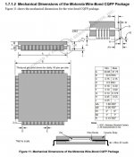
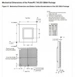
Poked around in the docs, the BGA 740 will easily fit atop a CQFP adapter with room to spare for what not. Maybe not enough stuff, but maybe?


Franklinstein

Well-known member
A quick comparison of the relative sizes of a ZIF module's PGA and the 601 suggests that it would be difficult to build a QFP-to-ZIF adapter, unless there's a BGA version of the ZIF socket available (I've only ever seen through-hole). So that may not work.

I'm pretty sure any of the BGA PPC chips would fit well within the confines of a QFP adapter along with a few very small support devices. Worst case you can run some wires to it from an external power regulator if necessary. With that, maybe it would be possible to use a 750CX or 750FX? That way you get your L2 cache and potentially higher clocks (the CX and FX support more than a 10x bus multiplier).


Trash80toHP_Mini

NIGHT STALKER
Dunno about the Cache setup of the 750 other than the higher pin count of that version for the Cache interface. The Cache subsystem might be documented in one of the manuals above. That stuff is waaaay beyond my ken. If it's documented, cache may be a very remote possibility, but if not, I'd say not. Dunno, haven't looked beyond taking a couple of dimension screen shots for reference.

PPC740-BGA-Dimensions.JPG

Fitting a 21mm BGA 740 onto a 35mm adapter with the bus multiplier resistors and a bit of other cruft looks doable.

CQFP 603e Dimensions.JPG

I like your notion of moving any 3.3V crud off the adapter. :approve:


Franklinstein

Well-known member
Right, so the 750 has more pins than the 740 because it has the L2 cache interface, but the 740 could possibly (if it as the capability) use the bus-level L2 cache originally equipped to the x100 machines. The 740 is designed to be pin and signal compatible with the 603e, and the 603e is often equipped with a bus-level L2 cache of some sort, so you'd think the 740 would also operate with one. Apparently there were 1MB cache modules available for the WGS models but I don't think I have ever seen one.

As for later chips, the 750CX has a 256k L2 cache, the 750FX a 512k L2 cache, and the 750GX a 1MB L2 cache, all on-die at full processor speed. Because it's on-die, the L2 cache should always be on and available by default, which should avoid the need for any of the L2 cache extensions used by typical G3 upgrades. Plus, these chips would not require the external cache chips or associated support devices, the lack of which would undoubtedly simplify a project like this. Also these chips run from 400MHz-1.2GHz, depending on which model is used, while the basic 750 generally tops out at 500MHz. I don't know if the 750CX has ever been used in an upgrade of any sort; any >500MHz G3 upgrades I have seen have used FX or GX chips.

It looks like the best idea would be to use a QFP-to-BGA adapter with a 750FX on top along with a DIP switch arrangement for speed selection, and an external VRM that plugs into one of the disk drive power connectors. The only unaddressed problem that remains is heat management: the stock heat sink will no longer fit properly (nor will it likely be adequate). Some G3 upgrades (PowerLogix, I think) used a type that clipped directly to the processor and twisted to tighten. That would probably be the best approach here, if a source of these heat sinks was found. The only other solution would be thermal adhesive of some sort to permanently attach a generic heat sink.


Trash80toHP_Mini

NIGHT STALKER
I wasn't aware of the faster, on-board cache CPUs. If a CQFP SMT pad to BGA adapter PCB can be developed one could make my 2300c run nice and toasty.


trag

Well-known member
Yeah, the 750CX is still fairly available.   Good luck finding stock of the 750FX or 750GX at a not-crazy price.     I think the 750CX only goes up to about 400 or 500 MHz, but I might be wrong.

I wish I had had $10,000 laying around back when the 750GX was in production.   I would have picked up 100 of them....   Of course, I wish I had $10,000 laying around now too....


Trash80toHP_Mini

NIGHT STALKER
Money woulda' been better spent on Apple stock, whodathunkit?

A 400-500MHz 750CX would be nice to try in my Duo 2300c and the 6290 which has a cache SIMM. It's lowend NuBus architecture, so nobody ever looked at that slot, much less the machine for accelerator development. I wonder which package CPU is in my 5300c? ce version's BGA IIRC. That would be fun to look at, as well as the 3400c.

Are the ZIF processor cards in the BeigeG3 straight up Motorola parts? Looks kinda like that from the docs I've dug up.


trag

Well-known member
Okay. looks like Quest Components has forty-eight 600 MHz 750CX for ~$20 each.  The 750cx comes in a 256 pin BGA (27mm X 27mm).   Bus multiplier only goes up to 10X, which is probably why I was thinking it was limited to 500 MHz.   On a 50MHz bus machine, the fastest you can run it is 10 X 50 = 500 MHz without overclocking the bus.

They have some (7) 750FX at  800 MHz for $32.50.  That's pretty good.   292 pin BGA (21mm X 21mm).   The 750FX has up to a 20X bus multiplier.

Anyone know how the 750GL differs from the 750GX?    They have 81 750GL for $34.50 - $39.    Same package as the 750FX and also up to 20X multiplier.   The GL has a 1MB L2 cache like the GX...


Trash80toHP_Mini

NIGHT STALKER
Nice! What do you think of the notion of doing as many layers as needed to adapt from the Duo's CQFP pads to BGA? With solder mask on mobo and adapter it looks like hot air might work?

Would the thickness of the two solder masks cause contacts on logic board and adapter to be too far apart to bridge in that manner? I figure I can grind some off bottom of the heat spreader if using a thinner thermal tape doesn't do the trick. If thickness of the adapter PCB brings the top of the CPU into contact, thermal compound between it and the heat spreader should work?

 
Last edited by a moderator:

Franklinstein

Well-known member
Money woulda' been better spent on Apple stock, whodathunkit?

A 400-500MHz 750CX would be nice to try in my Duo 2300c and the 6290 which has a cache SIMM. It's lowend NuBus architecture, so nobody ever looked at that slot, much less the machine for accelerator development. I wonder which package CPU is in my 5300c? ce version's BGA IIRC. That would be fun to look at, as well as the 3400c.

Are the ZIF processor cards in the BeigeG3 straight up Motorola parts? Looks kinda like that from the docs I've dug up.
The 603e's QFP is probably about 10% smaller than the 601, which would make any adapter a little harder to work with. Still possible, but you'd have less space for discrete devices or switches or anything like that.

All of the 52/53/54/62/63/64xx series machines used QFP 603/603e chips, including the PCI models. The 44/55/6500 series and the TAM used BGA 603e chips. The PowerBook Duo 2300 and all variants of the 5300 use QFPs, the 1400 will use either QFP or BGA, and all 24/3400 models use BGA processors. So a QFP-to-BGA adapter with a faster chip is possible in some of these but in the ones that used BGA processors, the only option is to use a PPC 740, which generally topped out around 300MHz. The reason is that the PPC 740 is pin compatible with the 603e, but none of the 750s are. 

The 3500/original G3 is already a BGA 750, but it's theoretically possible to swap the 250MHz chip out with a 500MHz part (assuming the 750L is pin-compatible with the 750, which it should be). Of course you would also have to consider the L2 cache: do you replace it at the same time with larger and/or faster cache chips, or configure it to run at a lower multiplier?  I don't think the original cache chips could run at double their original speed if paired with a 500MHz processor. 

The biggest concern with PowerBook use of a QFP-to-BGA adapter would be the thickness of the total package. It's possible to do if the thinnest substrate was used for the adapter and a 750CX was mounted to it (it's the smallest of the 750s in terms of total package height). The 603e may already use voltages that are usable by the 750CX, which would greatly simplify the design of an adapter and reduce the requirement for support devices. Of course a Duo 2300 or 5300 would be limited to 333MHz if the 750CX's max of a 10x multiplier is correct, but that's still over 3 times faster than stock.

I'm not sure where the design originated, but IBM was using the same ZIF socket in their RS/6000 models before the beige G3 was introduced. A good number of the early ZIF G3 cards that I've seen have had Motorola tags on them and "MOTO97RISC" somewhere on the bottom in the substrate.


Trash80toHP_Mini

NIGHT STALKER
From the data sheet on the 750, it appears to be a ZIF part with CPU and cache on board as a stock config. straight from the mfr.

Data sheet above says the 740 BGA is a 21mm square on top of the 34.6+mm square of the CQFP legs and out to near the edge of the pads, plenty of room.

In the Duo there would be four tiny resistors for the multiplier, no switches. Don't even need to find the native multiplier resistors (something I've been whittling away at for some time) as you'd have a disconnect from those legs on the adapter. Looks like you'd need to stash a voltage regulator somewhere and place caps around the edge of the BGA package for the 3.3V supply.

In the spec pages above, BGA package of the 740 is .65mm lower than the CQFP 603e. Like I said, thickness of the thermal tape on the 603e provides more slack needed for adapter thickness.

@tragdo those later versions of the 750 have on die cache or are they assemblies in a BGA package as opposed to ZIF? I found a data sheet, but couldn't find config diagrams.


Trash80toHP_Mini

NIGHT STALKER
Was wondering about that solder mask induced gap between an adapter PCB's contacts and the CPU pads on the mobo. I remember talking about using the temperature differential between leaded and ROHS solder to bake SMD components onto both sides of a board. Might tinning the contacts of the adapter with the higher melting temp solder make up the gap and stay in place well enough to use the lower temp type via hot air method for installation?

The 750GX has only one contact more than the 740, that's why I'm so curious about the package dimensions. The cache would almost have to be on die per the info you posted. Might the 750GX & GL remain signal compatible with the 603e? If so, I'm also wondering if a maximum trace length difference across such a small adapter PCB could be a problem at 25MHz? Meandering would be a major PITA.

 
Last edited by a moderator:

trag

Well-known member
Original PPC750 was in a 360 pin BGA (25mm X 25mm) with 8X maximum bus multiplier and selectable IO voltages of 3.3V, 2.5V or 1.8V.

PPC750L raised maximum bus multiplier to 10X.   These are the "copper" G3s.  360 pin BGA (25mm X 25mm)  

PPC740L     As above, but in 255 pin BGA (21 mm X 21 MM).    I guess this is the PPC603 compatible package, but not certain.

PPC750CX   Moved L2 cache to on-chip.   256K L2 cache on-chip.   Up to 10X bus multiplier.   256 pin BGA (27mm X 27mm)

PPC750FX   L2 cache increased to 512KB.  up to 20X bus multiplier.   292 pin BGA (21 mm X 21 mm)

PPC750GX, as 750FX except on-chip L2 cache increased to 1 MB.

I have not looked at the pinout, but given the different package sizes, I don't think the 750CX could be compatible with the PPC740/PPC603.

 
Top