• Updated 2023-07-12: Hello, Guest! Welcome back, and be sure to check out this follow-up post about our outage a week or so ago.

ROMBUS - 64 MB flash interface for Mac Plus

ZaneKaminski

Well-known member
Hi 68kMLA,

Maybe some people here remember my ARM-based "Maccelerator" proposal from a few years ago. I have cost-reduced the BOM for that project significantly and plan to get the hardware released soon, but that's not for today. Since the Maccelerator proposal, I have been working with a friend of mine, Garrett Fellers, and we have been selling an Apple IIGS memory expansion under the Garrett's Workshop brand. People seem really pleased with that card, so we are trying to get some more of my designs out there. I have a ton of vintage product designs in the backlog which I really wanna release. My post today is about one of them, which we call ROMBUS (or GW4101). It's a 64 MB flash disk interface for Macintosh Plus, replacing its two socketed DIP ROM chips:
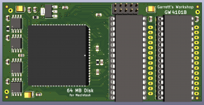
ROMBUS-B.png

The original inspiration for the project was Big Mess O' Wires' Mac ROMinator. When I heard it was being discontinued, I tried to come up with a worthy replacement. ROMBUS implements a 16-bit-wide interface to four SPI flash memory chips. The idea is to get the flash chips into quad read/write mode, in which four bits can be read or written at once from each of four flash memories, thus making a 16-bit interface. ROMBUS interfaces with Mac Plus via the Mac's two ROM sockets. To store a patched toolbox ROM with the flash driver, there are two sockets on ROMBUS which can each accommodate a 512 kilobyte flash ROM, making a total of 1 MB of parallel flash ROM. The Mac Plus has 128 kB of ROM, but can address 256 kB through the sockets, so bank-switching is required to access the total 1 MB capacity. Because the R/W signal is not sent to the ROM socket, writing to the 64 MB serial flash and 1 MB parallel flash is accomplished by bank selection.

I have had boards for this project in hand for 6 months or so, and the CPLD programming is done too, save for any tweaks or bug fixes:
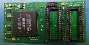
IMG_0848.JPG

Actually, this is the second revision (GW4101B). The first revision (GW4101A) is basically electrically identical, so the same driver and CPLD programming will work on both, but the flash memory land patterns are wrong, so the GW4201A one can only accommodate 16 MB serial flash despite the board advertising itself as a "32 MB Disk."

I will be releasing the design files for this product soon, under some kind of open-source license, probably GPL, so anyone can make (or sell) their own, or make improvements. We (at Garrett's Workshop) have just finished our SMD assembly line, and we will be selling the card for $40 USD, shipped to the US. Not sure if many will purchase it, since BMOW says his ROMinator was not too popular, but the price strikes me as fair, and I am pleased to have eliminated the need to jumper the R/W signal and the couple of address signals like you have to in order to install the ROMinator. We have 20 of the 64 MB boards, but I want to gauge the interest to see if I oughta order more in preparation for a product launch. 

Now, what I need help with is the driver. I have looked at the drivers for the ROMinator and BBraun's previous work, but the way to access the flash memory is different, plus there oughta be a wear-leveling scheme to minimize erase time overhead and maintain the endurance of the flash. (I have a fair solution for the wear-leveling but it takes 256 kB of memory for a 64 MB disk.) My hope is that some other skilled members of the community can assist with the driver development, and then the whole thing can be put onto GitHub for others to build themselves, improve, learn from, etc. And of course we will sell the boards for $40 each, which we think is fair.

So, does anyone want this? Is it fair to ask for assistance on this when we are trying to make some money on sales of the product? And if so, who can assist a little with the driver development? Just pointing me in the right direction in terms of what development tools to use, environment setup, etc. would be really appreciated. Of course, free hardware will be provided to the top contributors. Looking forward to hearing what everyone thinks.

 
Last edited by a moderator:

maceffects

Well-known member
@ZaneKaminski looks interest, I’d buy one or two once your at that point.  Love the idea of this.  Also, I contacted Garret asking if he would be interested in helping with our LC to SE/30 PDS adapter project. Once that is complete we can integrate WiFi.  I’m happy to offer payment. If you could chat with him about that, I’d appreciate it.  


Byrd

Well-known member
I'm interested - you'd significantly broaden your market if it worked in a 128K, 512K ... or SE?


ZaneKaminski

Well-known member
I will proceed more quickly then since there is interest!

Hopefully someone with some experience in driver development for the classic Mac OS can come along. I've read Inside Macintosh, but, unless I missed something, there isn't much about how to install a new driver in the system, though there is a lot about what kind of calls can be made to a disk driver. Also, what kind of development environment is best? I am not sure if I should be trying to develop the driver in Mini vMac or if I should go the unix route and build it in Linux/OS X with a crosscompiler. Does anyone have any experience with this?

@LaPorta, it's sort of like a ROM disk but it's also writable, so that makes it an SSD. Sorry if my first post was a little unclear or technobabbley, sometimes I get a little too deep into this stuff. Since Mac Plus doesn't have the capability for an internal hard disk, I wanted to make a fast internal disk that would allow a Plus to boot up an install System 6 with lots of apps and games and stuff. A ROM disk is okay but it would be even better to be able to change the disk from the Finder in the normal way.

@Byrd I eyeballed it and thought it would work in a Macintosh SE, but unfortunately the SE has its ROM sockets slightly further apart than the Plus, something like 0.025" further from each other, so a new board would be required to for it to fit properly in an SE. But it's of course doable. The 128k and 512k have a different ROM spacing too, but that's not the biggest problem. The difficult thing is that their RAM is so limited. The driver I had planned needs to store a total of 256 kB of data. Most Pluses have 4 MB of RAM so that's not too bad in exchange for such a fast boot disk, but obviously the earlier Macs can't do it.

@maceffects Yes, you and I talked as well. I was going to do a quick board for you to do the requisite address mapping to access the LC PDS card properly in an SE/30, but it sort of slipped my mind as other things came up. You guys should skip right to making a board. PCBs are cheap these days, especially if visual quality isn't critical, as is the case with a prototype. Many PCB vendors will sell you 10 boards of the size you need for $10, then there's shipping which might even be 10-15 more, but hey, if your design works, you have a working, reproducible prototype really easily. I never spend much time in the prototyping stage. Instead I read the manuals and study the existing products that are similar to my design to verify that I'm on the right track. And if your design is wrong, just cut and jumper to make it work, then change that in the PCB and spend another $20 to get the board remade. It's so much easier than wire-wrapping or whatever. If you design a PDS adapter board, I'll check it over and include your it in my next board fabrication order. My plate is really full so I can't really take it on. I just announced a five new Apple II cards on AppleFritter (not much traction over there though), so I've gotta work on finishing those.

 
Last edited by a moderator:

LaPorta

Well-known member
Sign me up. That was what I was hoping it was, and it sounds like a wonderful, practical idea!


maceffects

Well-known member
@ZaneKaminski Thanks for the information.  We are actually stick with the video issue in slot $E.  Making a simply adapter is not possible, we must over come that issue first.  I know other cards did overcome the issue, but haven't figured it out.  Maybe @Bolle and @Trash80toHP_Mini can chime in of the specifics holding the project back.  Should you have any time to assist with this project, I'm happy to officer a considerable amount for your time, you'd be surprised :cool:

AppleFritter is great but has a small audience.  Have you tried the forum at http://vintage-computer.com/ this is a good place.  As well as the Apple II Enthusiasts Facebook page.  I know there are others but I am just learning about the Apple II community better from my Apple II case project. 


Gorgonops

Moderator
Staff member
So, to be clear I don't intend this as a criticism, but I am curious: if the storage on the 64MB flash you're adding is accessed like a "disk", what is the advantage of your design compared to hanging, say, an interface to an SD card controller off the ROM sockets? From an API standpoint SD cards present a "SCSI-like" storage interface and you get whatever rudimentary wear-leveling the manufacturer sticks on the card for free.

(Flip side is it would probably be painfully slow if you had the Mac running the card via SPI itself through minimal glue, although, honestly, if it at least presented itself as a buffered 8-bit port and didn't require the CPU to bit-bang everything it may well be as fast as the Plus' built-in SCSI controller.)


ZaneKaminski

Well-known member
@Gorgonops Yes, there is a good reason to use SPI flash instead of an SD card. The goal was to make the fastest disk possible. If I want to move 16 bits off of an SD card, I need to have a clock going faster than the CPU transfer rate to serialize the data, plus more macrocells and routing resources in the CPLD to buffer the data. And since no clock signal is sent to the ROM socket, I’d have to have an even faster clock on the card and then synchronize the inputs coming from the Mac. So the SPI flash is easier since you can reasonably put 4 and work them all in parallel to make a 16-but port, at the expense of a smaller capacity and the need to wear-level

So the aim is to bit-bang but to be able to read data at maximum speed once the proper bits have been twiddled to submit the command and address. This struck me as the easiest way to do that.

 
Last edited by a moderator:

ZaneKaminski

Well-known member
@LaPorta Thank you, but there’s no need! I’m pretty sure this hardware is gonna work, and I’ve been sitting on boards and parts for a while. I’ve gotta make the driver, verify the sort of low-level hardware programming in the big chip, and then make the boards. Little additional expense is involved.

@GorgonopsOne more thing on the subject of clock signals and timing, there is a somewhat unusual element (some would even say it’s bad practice) to this board insofar as how it generates the clock signal to be sent to the SPI flashes. For read operations, data must be clocked out of the flash sort of in the middle of the read cycle. What I mean is that the 68000 asserts /AS and /LDS/UDS and then that in turn causes the ROMs to be selected. Somehow, as a consequence of the single falling edge of the ROM’s select signal, a clock pulse with a width of 10ns or so must be sent to the flash. This is generated by a little RC network in conjunction with the CPLD. The RC network is carefully chosen to meet the minimum pulse width spec of the flash as well as the maximum rise time spec of the CPLD. The need for this self-timed circuit is another consequence of not having the clock signal at the ROM socket, or else I’d have to have a faster oscillator always running on the board, and synchronize the inputs. It’s not clear that such a design would fit in the CPLD. 128 macrocells sounds like a lot, but there are fan-in limitations so a bus-oriented design rarely achieves full macrocell utilization in my experience compared to some random logic-type functions. 


Gorgonops

Moderator
Staff member
@GorgonopsOne more thing on the subject of clock signals and timing, there is a somewhat unusual element (some would even say it’s bad practice) to this board insofar as how it generates the clock signal to be sent to the SPI flashes...
Okay. Well, I mean if it looks like it's going to work I'm in no position to criticize. I do have to admit something does make me just a *little* leery, though; I googled up an application note for these quad-SPI flash chips, and this is what I got:

https://www.st.com/content/ccc/resource/technical/document/application_note/group0/b0/7e/46/a8/5e/c1/48/01/DM00227538/files/DM00227538.pdf/jcr:content/translations/en.DM00227538.pdf

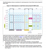
The application note talks about running these chips in parallel; it doesn't have an example of four in parallel, but it does have one for two. This diagram has me scratching my head:

image.png

Maybe I'm missing something, but the implication I get from this is that the way the memory cycle works with these things is that when you "go wide" with multiple packages it still expects each chip to send and receive a full "byte". IE, the data cycle is going to send two sets of four bits across the I/O lines as a unit. I don't find anywhere in this manual where it talks about the chip acting like it's only composed of four bit "nibbles" which are individually accessible. So if you have four of them in parallel (IE, "16 bits" worth of quad-SPI lines) won't you actually be pushing 32 bits per data cycle? Not that it would be something you couldn't handle, since you're planning on driving this with software on the 68000 instead of depending on this to just "transparently" look like ROM or a disk.

Anyway I think mostly what I had in mind when I suggested the SD thing was, given the aforementioned limits on the signals you have access to on the socket, was implementing the port in the form of a "mailbox" buffer between the Mac and a self-clocked MCU that actually handled the communication with the SD card. (Or, actually, in this scenario an MCU that can act as a USB host might be better? Something like a PIC 24FJ64GB00x?) That'd let it run asynchronously from whatever the Mac is doing, all you'd need is a register to communicate a "busy/ready" flag. Ultimately I think something like that would be stuck with performance somewhere in the same ballpark as the Mac Plus' built in SCSI controller. (Which also communicates entirely by polling in that machine.) So maybe there's no point. (Might be a fun upgrade for a 512k?)

I'm not sure off the top of my head what would really benefit from "lightning fast" bulk storage throughput in a Plus but it's certainly an unfilled niche. So by all means go for it.

 
Last edited by a moderator:

ZaneKaminski

Well-known member
@GorgonopsYes, although each device reads out 4 bits at once, you have to specify a byte address to each flash, and then there are four in parallel, so yeah, an address as sent to the SPI flash chips refers to a 32-bit data word. But like you said, it doesn't matter, since we can just write the driver to handle the addressing correctly, plus I believe the API we need to implement concerns itself with 512-byte sectors anyway. My aim with this project is to have a really quick boot time on a Plus, even faster than from floppy or a SCSI disk, and insignificantly slower than the ROMinator-type ROM disks.

The MCU approach is very workable, but I wanted to minimize the number of software pieces for this project. More software always means more bugs, whereas it's easier to iron things out with hardware in my opinion. I also wanted to eliminate the need for the Mac to busywait or poll a register in the course of a read operation. (For write operations, the driver must poll the SPI flash to see when the operation is complete, but I believe the time required for that is less than the seek time of a typical SCSI drive, so it's not too bad.)

If you're interested, I did use the MCU approach recently on two Apple II cards for which I have just finished the hardware, "Mouserial" and "Library Card."

Mouserial implements an Apple II mouse card with a PS/2 mouse interface. There is an AVR microcontroller on the card in conjunction with a CPLD. The CPLD's main function, other than some decoding and generation of select signals, is to implement a few dual-port registers. The AVR runs at 7 MHz, synchronous with the rest of the Apple II, and frequently polls the CPLD's dual-port registers to check if any new commands have been deposited in the command register by the 6502. The AVR interleaves polling the dual-port registers with bit-banging PS/2 such that the registers are polled whenever the AVR must wait in the context of bit-banging PS/2. If there is a new command, the AVR services it and updates the result and status registers in the CPLD. Meanwhile, the 6502 in the Apple II polls the status register to wait for completion of the command. This way is good for low-bandwidth applications, and the implementation of the dual-port registers in the CPLD was made easier by the fact that I could run everything from the same clock. The CPLD always latches write data into the dual-port registers at the end of PHI0, whereas the AVR has an extra wait state and the CPLD makes sure not to write the AVR's data at the same time that the 6502 is reading or writing. (That's sort of a simplification but it provides the gist of it)

Library Card interfaces the Apple II to an ESP32-based WiFi/Bluetooth module. The ESP32 has dual cores and can run at 240 MHz, so I did the bus interfacing differently on this one. In the CPLD, I buffered the data bus and part of the address bus to the ESP32, as well as sent it a select signal. Since the ESP32 is fast and has dual cores, it is just barely possible to poll a select signal in software and input/output data just fast enough to satisfy the 6502's timing. The polling loop has to be run all by itself on the second core, with no scheduler or OS getting in the way. That allows any arbitrary interface to be implemented. Honestly, I don't really know what I should be doing with this card in terms of drivers and software, so I thought that this type of busy-waiting implementation would be the most flexible, at the expense of using a whole core of the ESP32.

So the MCU approach isn't foreign to me. I just figured the dumber way is best. Also, a lot of people had this criticism of my ARM-based "Maccelerator" proposal, that it was too new, what with the ARM and the emulation and all, not to mention complicated. I wanted to keep this thing as simple as possible.

 
Last edited by a moderator:
Top