Note:
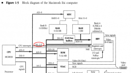
Concerning the mystery signal on pin A1 (reserved) on the PDS30 in the IIsi, which is connected to the PAL pin5. From DCaDftMF:
Pin A1 on the IIsi expansion connector is /RBV - An active-low chip-select signal for the RAM-based video IC. This signal can be used, along with further decoding, to enable signals for a cache circuit.
/CacheEnable(low) = /RBV • /RW • /A0 • /A1 • /A4 • /D0
/CacheEnable(high) = /RBV • /RW • /A0 • /A1 • /A4 • /D0 + RESET
/CacheFlush (low) = /RBV • /RW • /A0 • /A1 • /A4 • /D3
/CacheFlush (high) = /RBV • /RW • /A0 • /A1 • /A4 • D3
where • is Logical AND, + is Logical OR, and D0 is the logical complement of /D0
All other combinations of inputs should not affect the /CacheEnable or /CacheFlush outputs. The /CacheEnable signal should be set low when writing a 0 to bit 0 of the RBV register 0, and should be set high when writing a 1 to bit 0 of RBV register 0, or when the RESET signal is asserted. The /CacheFlush signal should be set low when writing a 0 to bit 3 of the RBV register 0, and should be set high when writing a 1 to bit 3 of RBV register 0, or when the RESET signal is asserted.
I think I just cracked the B5.oe equation.


